Display device and method for manufacturing the same

a technology of display device and manufacturing method, which is applied in the direction of sustainable manufacturing/processing, identification means, instruments, etc., can solve the problems reducing manufacturing yield, etc., and achieves the effect of reducing display quality and reliability, and reducing manufacturing yield

Active Publication Date: 2015-06-04
SEMICON ENERGY LAB CO LTD
View PDF0 Cites 87 Cited by
  • Summary
  • Abstract
  • Description
  • Claims
  • Application Information

AI Technical Summary

Benefits of technology

[0009]In a process of manufacturing a flexible display device, a minute defective portion that is not a problematic part when a rigid substrate is used may increase, which may reduc...

Problems solved by technology

In a process of manufacturing a flexible display device, a minute defective portion that is not a problematic part when a rigid substrate is used may increase, which may reduce ...

Method used


Image

  • Display device and method for manufacturing the same
  • Display device and method for manufacturing the same
  • Display device and method for manufacturing the same

Examples


embodiment 1

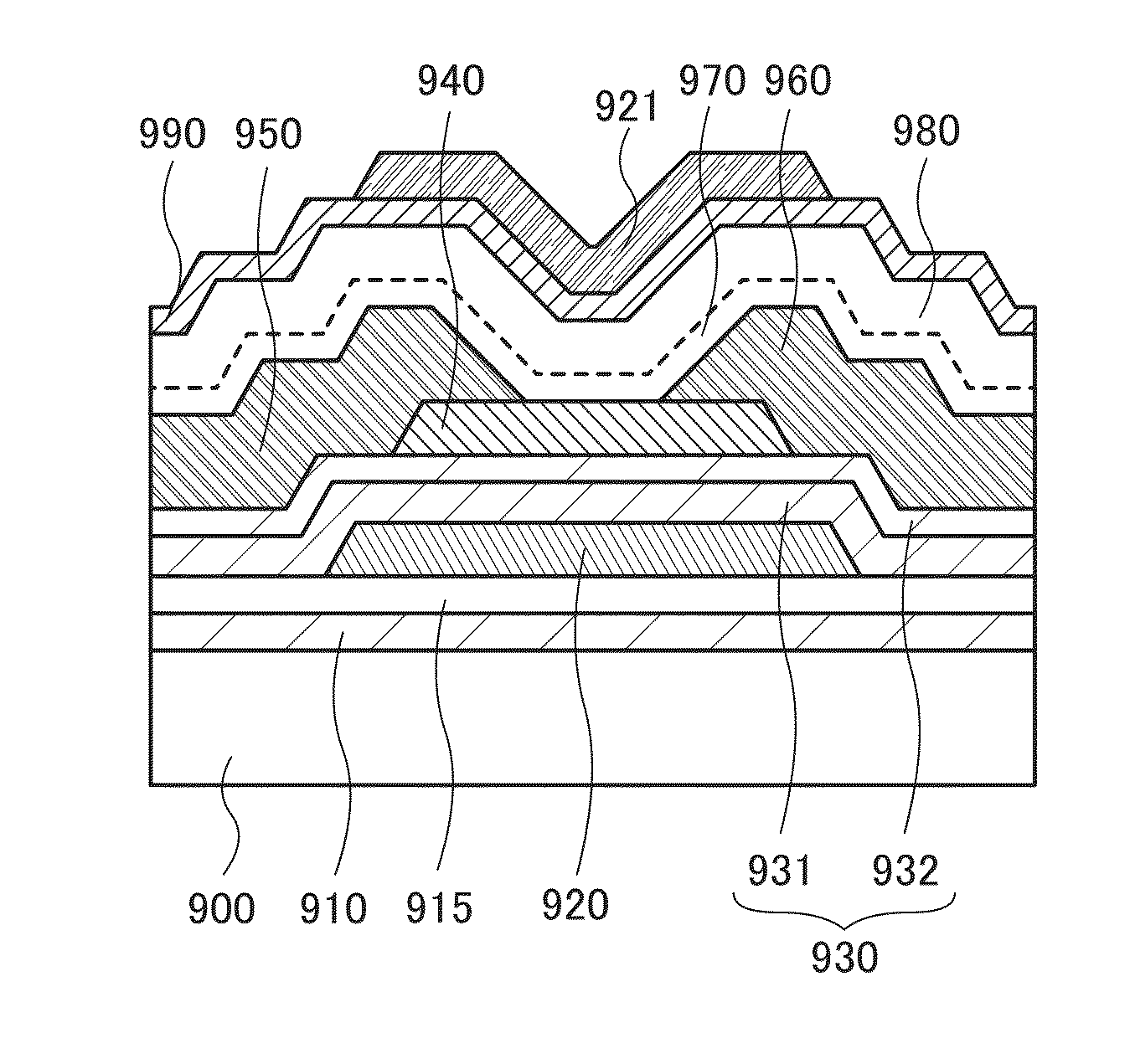
[0085]In this embodiment, a display device that is one embodiment of the present invention and a manufacturing method thereof will be described with reference to drawings.

[0086]The “display device” in this specification means an image display device or a light source (including a lighting device). Further, the display device includes any of the following modules in its category: a module including a connector such as a flexible printed circuit (FPC), or tape carrier package (TCP); a module including TCP which is provided with a printed wiring board at the end thereof; and a module including a driver circuit which is directly mounted on a display element by a chip on glass (COG) method.

[0087]The display device that is one embodiment of the present invention has flexibility (flexible display device). Note that “flexible device” means that a device that can be bent or warped. The flexibility can be utilized in an end product in some cases and utilized in a manufacturing process in some...

embodiment 2

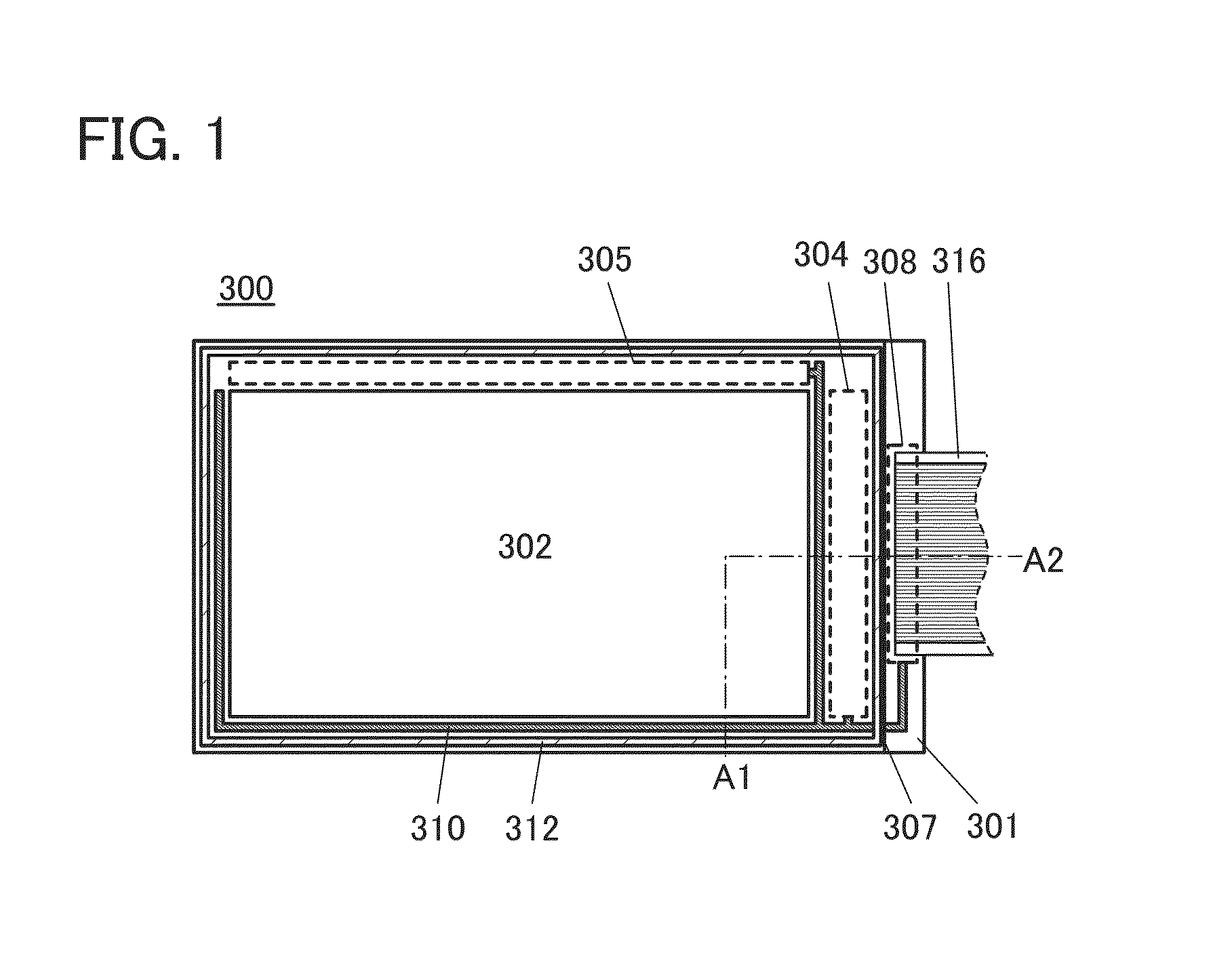
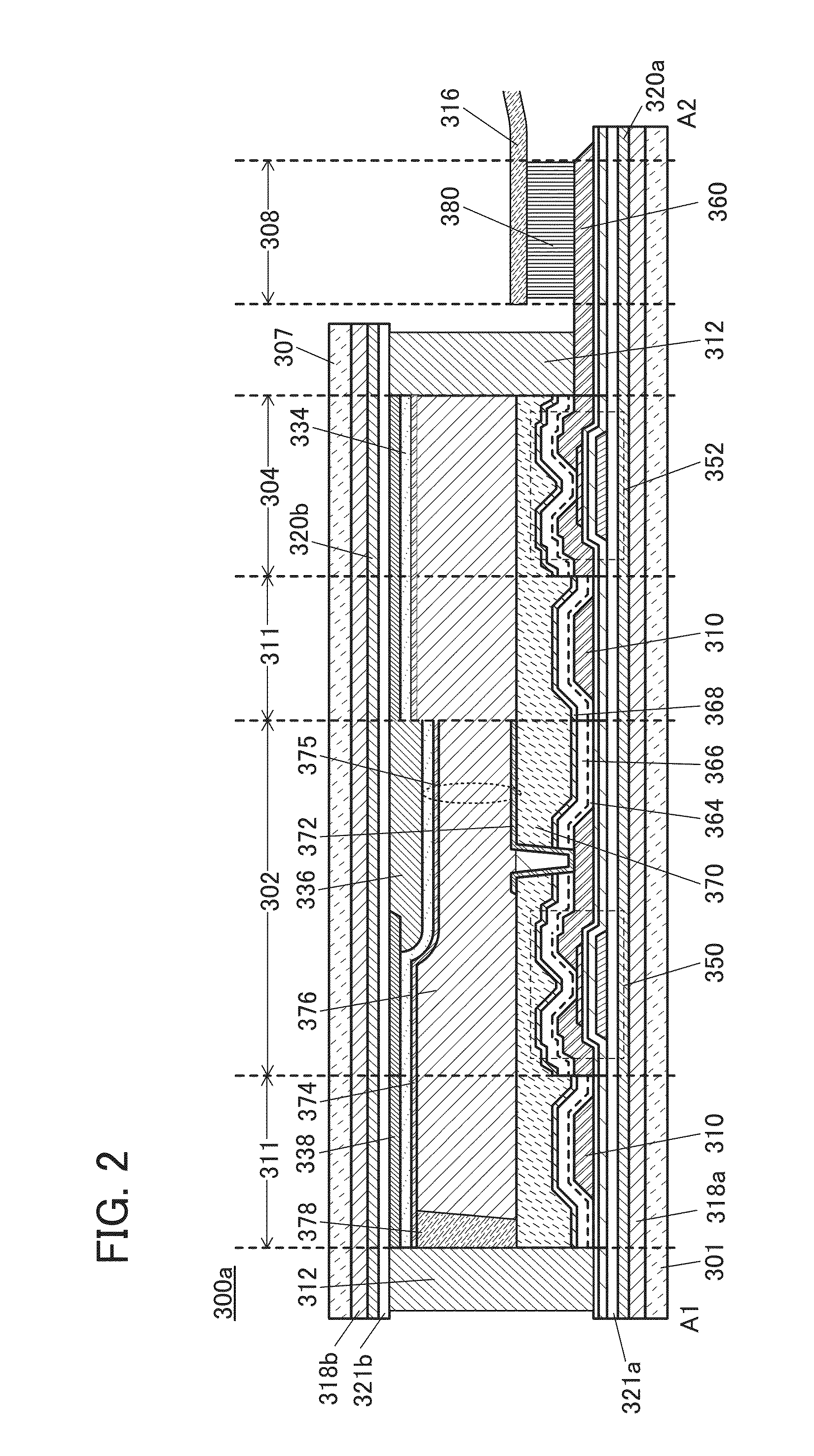
[0171]In this embodiment, a separation apparatus of one embodiment of the present invention will be described with reference to FIGS. 7A to 7D, FIGS. 8A to 8C, FIGS. 9A to 9C, FIGS. 10A to 10E, FIGS. 11A to 11C, FIGS. 12A to 12C, FIGS. 13A to 13C, and FIGS. 14A and 14B. One embodiment of the present invention is a separation apparatus including a structure body that can hold a first member of a processed member, and a stage that can hold a second member of the processed member. With the separation apparatus, the processed member between the structure body and the stage is separated into the first member and the second member while the first member is rolled up. For example, the first member corresponds to the stacked body other than the second substrate 463 illustrated in FIG. 5A, and the second member corresponds to the second substrate 463.

[0172]With the separation apparatus of one embodiment of the present invention, the processed member can be separated into the first member and...

structure example 1

[0174]With reference to FIGS. 7A to 7D, FIGS. 8A to 8C, and FIGS. 9A to 9C, an example in which a first member 103a is peeled from a processed member 103 to separate the first member 103a and a second member 103b is shown.

[0175]FIG. 7A is a perspective view of a separation apparatus just before the peeling is performed, FIG. 7B is a front view thereof, and FIG. 7D is a side view thereof.

[0176]The separation apparatus illustrated in FIGS. 7A to 7D includes a structure body 101 and a stage 105. The structure body 101 has a convex surface. The stage 105 has a supporting surface facing the convex surface.

[0177]In FIGS. 7A to 7D, the processed member 103 is arranged between the convex surface and the supporting surface of the separation apparatus.

[0178]FIG. 7C is a top view showing a case where a position of the processed member 103 with respect to the structure body 101 is different from that in FIG. 7A, FIG. 7B, and FIG. 7D. FIG. 7A shows the case where the peeling starts at a side por...


PUM

PropertyMeasurementUnit
Compositionaaaaaaaaaa
Adhesion strengthaaaaaaaaaa
Flexibilityaaaaaaaaaa

Abstract

A first organic resin layer is formed over a first substrate; a first insulating film is formed over the first organic resin layer; a first element layer is formed over the first insulating film; a second organic resin layer is formed over a second substrate; a second insulating film is formed over the second organic resin layer; a second element layer is formed over the second insulating film; the first substrate and the second substrate are bonded; a first separation step in which adhesion between the first organic resin layer and the first substrate is reduced; the first organic resin layer and a first flexible substrate are bonded with a first bonding layer; a second separation step in which adhesion between the second organic resin layer and the second substrate is reduced; and the second organic resin layer and a second flexible substrate are bonded with a second bonding layer.

Description

TECHNICAL FIELD[0001]One embodiment of the present invention relates to a semiconductor device including an oxide semiconductor, a display device including the semiconductor device, and a manufacturing method thereof.[0002]Note that one embodiment of the present invention is not limited to the above technical field. The technical field of one embodiment of the invention disclosed in this specification and the like relates to an object, a method, or a manufacturing method. In addition, one embodiment of the present invention relates to a process, a machine, manufacture, or a composition of matter. Specifically, examples of the technical field of one embodiment of the present invention disclosed in this specification include a semiconductor device, a display device, a liquid crystal display device, a light-emitting device, a lighting device, a power storage device, a storage device, a method for driving any of them, and a method for manufacturing any of them.[0003]In this specificatio...

Claims


Application Information

Patent Timeline
IPC IPC(8): H01L51/00H01L51/52H01L51/50H01L51/56
CPCH01L51/0097H01L51/56H01L2251/5338H01L51/5096H01L51/0027H01L51/5246G02F1/1303G09F9/33H01L27/1225H01L27/1251H01L29/78648H10K59/00H10K59/1213H10K59/1201H01L27/1266H01L29/78603H01L29/7869H10N30/074H10K59/38H10K59/12H10K71/50H10K71/421H10K71/80H10K77/111H10K50/8426H10K50/865H10K2102/311Y02E10/549Y02P70/50H10K59/126H10K50/844H10K59/124H10K71/00H10K50/18H10K2102/351H01L29/24H01L29/66969B23K26/0622B23K26/04B23K26/0617B23K26/0643B23K26/0648B23K26/083
Inventor YAMAZAKI, SHUNPEIOHNO, MASAKATSUADACHI, HIROKIIDOJIRI, SATORUTAKESHIMA, KOICHI
Owner SEMICON ENERGY LAB CO LTD
Why Eureka
Try Eureka