Semiconductor substrate and fabrication method thereof

Active Publication Date: 2015-06-25
SILICONWARE PRECISION IND CO LTD
View PDF2 Cites 2 Cited by
  • Summary
  • Abstract
  • Description
  • Claims
  • Application Information

AI Technical Summary

Benefits of technology

The present invention eliminates the need for an etch stop layer, reducing fabrication costs and simplifying the process. It also reduces the critical diameters of second vias and conductive vias, improving performance.

Problems solved by technology

In a flip-chip packaging process, a big CTE (Coefficient of Thermal Expansion) mismatch between a chip and a packaging substrate adversely affects the formation of joints between conductive bumps of the chip and contacts of the packaging substrate, thus easily resulting in delamination of the conductive bumps from the packaging substrate.
On the other hand, along with increased integration of integrated circuits, a CTE mismatch between a chip and a packaging substrate induces more thermal stresses and leads to more serious warpage, thereby reducing the product reliability and resulting in failure of a reliability test.
However, when fine circuits are formed on either the side of the silicon interposer facing the semiconductor chip or the other side of the silicon interposer facing the packaging substrate through a semiconductor process, the fine circuits easily delaminate from a dielectric layer, thereby reducing the reliability of the silicon interposer.
The etch stop layer made of such as silicon nitride generally has a high dielectric constant, which induces a large capacitance effect, such as an RC delay.

Method used


Image

  • Semiconductor substrate and fabrication method thereof
  • Semiconductor substrate and fabrication method thereof
  • Semiconductor substrate and fabrication method thereof

Examples


Embodiment Construction

[0035]The following illustrative embodiments are provided to illustrate the disclosure of the present invention, these and other advantages and effects can be apparent to those in the art after reading this specification.

[0036]It should be noted that all the drawings are not intended to limit the present invention. Various modifications and variations can be made without departing from the spirit of the present invention. Further, terms such as “first”, “second”, “a” etc. are merely for illustrative purposes and should not be construed to limit the scope of the present invention.

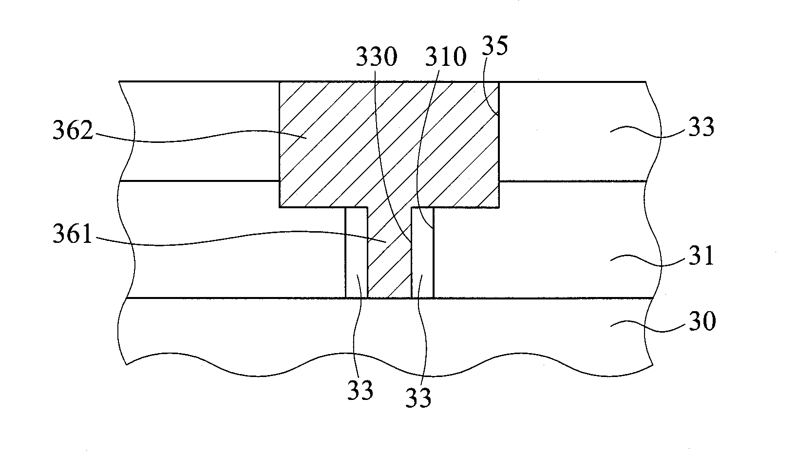
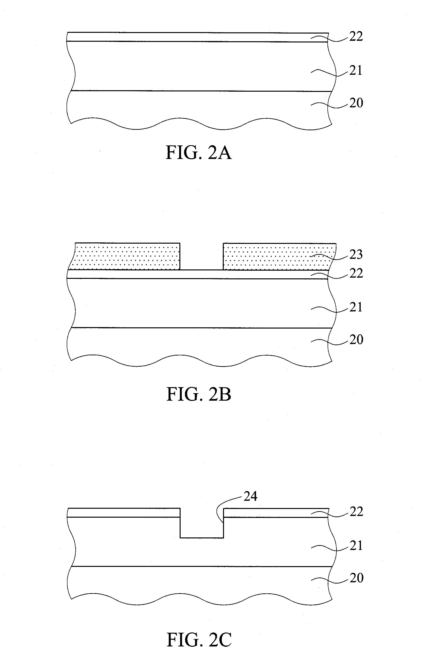
[0037]FIGS. 3A to 3I are schematic cross-sectional views showing a semiconductor substrate and a fabrication method thereof according to the present invention.

[0038]Referring to FIG. 3A, a first dielectric layer 31 is formed on a substrate body 30. The first dielectric layer 31 can be made of silicon oxide. The substrate body 30 can have circuits (not shown) formed thereon.

[0039]Referring to FIG. 3B, a first...


PUM


Abstract

A method for fabricating a semiconductor substrate is disclosed, which includes: forming a first dielectric layer on a substrate body; forming a plurality of first vias penetrating the first dielectric layer to expose portions of the substrate body; forming a second dielectric layer on the first dielectric layer and the exposed portions of the substrate body, wherein the second dielectric layer extends on walls of the first vias; etching the second dielectric layer to form a plurality of openings communicating with the first vias and form a plurality of second vias penetrating the second dielectric layer in the first vias so as to expose portions of the substrate body, leaving the second dielectric layer on the walls of the first vias; and forming a circuit layer in the openings, and forming a plurality of conductive vias in the second vias for electrically connecting the circuit layer and the substrate body.

Description

BACKGROUND OF THE INVENTION[0001]1. Field of the Invention[0002]The present invention relates to substrates and fabrication methods thereof, and more particularly, to a semiconductor substrate and a fabrication method thereof.[0003]2. Description of Related Art[0004]Flip-chip technologies facilitate to reduce chip packaging sizes and shorten signal transmission paths and therefore have been widely used for chip packaging. Various types of packages such as chip scale packages (CSPs), direct chip attached (DCA) packages and multi-chip module (MCM) packages can be achieved through flip-chip technologies.[0005]In a flip-chip packaging process, a big CTE (Coefficient of Thermal Expansion) mismatch between a chip and a packaging substrate adversely affects the formation of joints between conductive bumps of the chip and contacts of the packaging substrate, thus easily resulting in delamination of the conductive bumps from the packaging substrate. On the other hand, along with increased in...

Claims


Application Information

Patent Timeline
IPC IPC(8): H01L21/768H01L23/522
CPCH01L21/76879H01L23/5226H01L21/76802H01L23/53295H01L2224/16225H01L2224/73204H01L2224/32225H01L2924/0002H01L2924/15311H01L2924/00H01L21/76807H01L21/7681H01L21/76831H01L2221/1031
Inventor CHANG, WEI-CHE
Owner SILICONWARE PRECISION IND CO LTD
Why Eureka
Try Eureka