Microlens array, method for manufacturing microlens array, electro-optical device and electronic apparatus

Active Publication Date: 2015-07-09
SEIKO EPSON CORP
View PDF6 Cites 3 Cited by
  • Summary
  • Abstract
  • Description
  • Claims
  • Application Information

AI Technical Summary

Benefits of technology

The patent describes an electronic device that uses a special technology to efficiently display information. The device is designed to be bright and easy to read.

Problems solved by technology

However, the microlens array disclosed in JP-A-2011-158755 has a problem of a poor utilization efficiency of light.
Particularly, the problem is serious in the microlens array disclosed in JP-A-2011-158755, and even using a microlens array, there is a limit on the improvement in brightness.
In other words, in a microlens array of the related art, a problem arises in that it is difficult to sufficiently improve the utilization efficiency of light.

Method used


Image

  • Microlens array, method for manufacturing microlens array, electro-optical device and electronic apparatus
  • Microlens array, method for manufacturing microlens array, electro-optical device and electronic apparatus
  • Microlens array, method for manufacturing microlens array, electro-optical device and electronic apparatus

Examples


embodiment 1

Electro-Optical Device

[0045]An active matrix-type liquid crystal device including a thin film transistor (TFT) as a pixel switching element will be described as an example of the electro-optical device. The liquid crystal device is able to be suitably used as a light modulating element (liquid crystal light valve) of a projection-type display device (projector) described later.

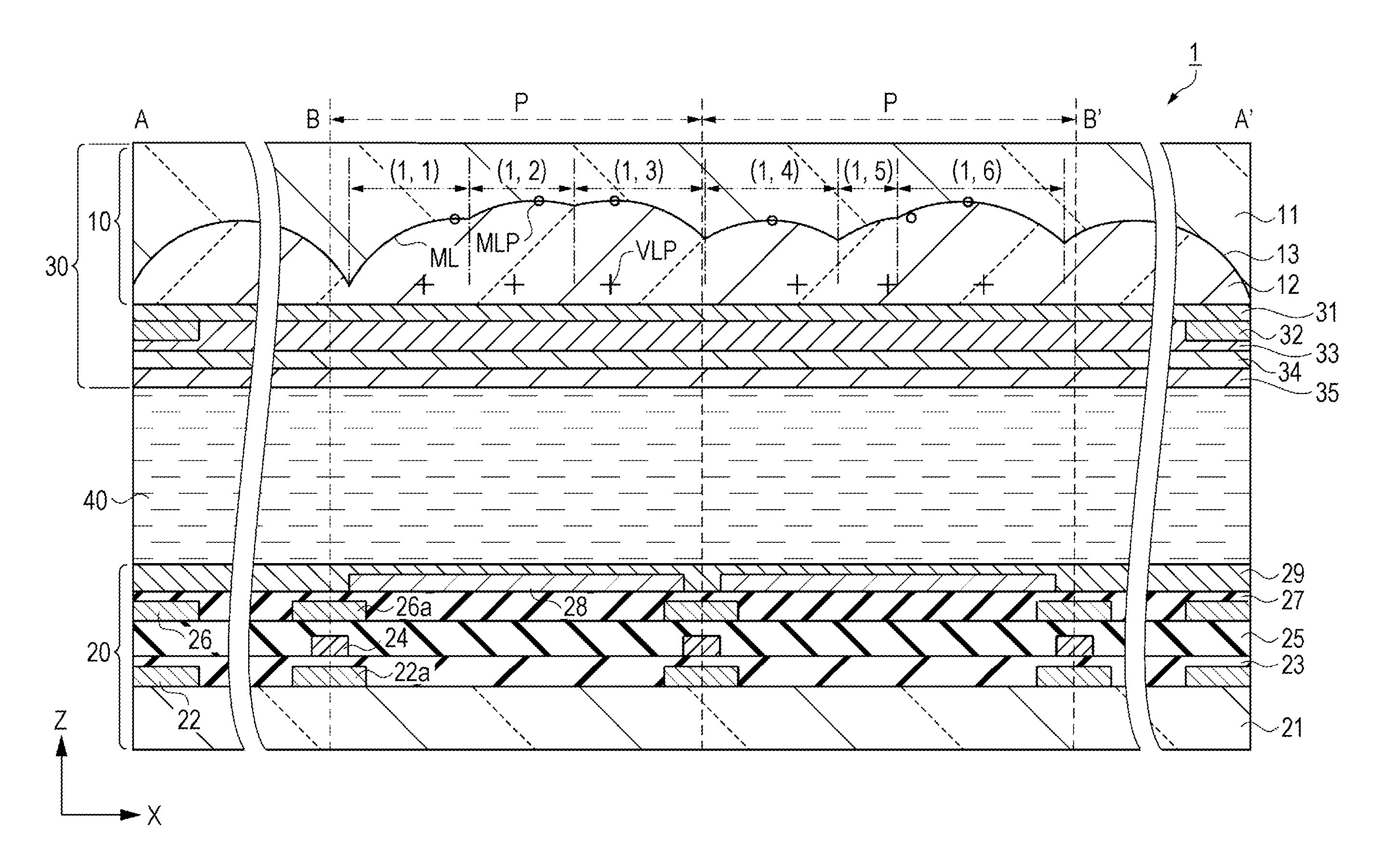
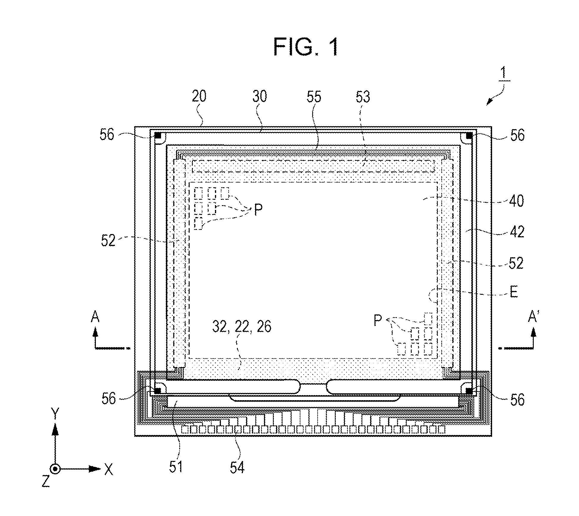
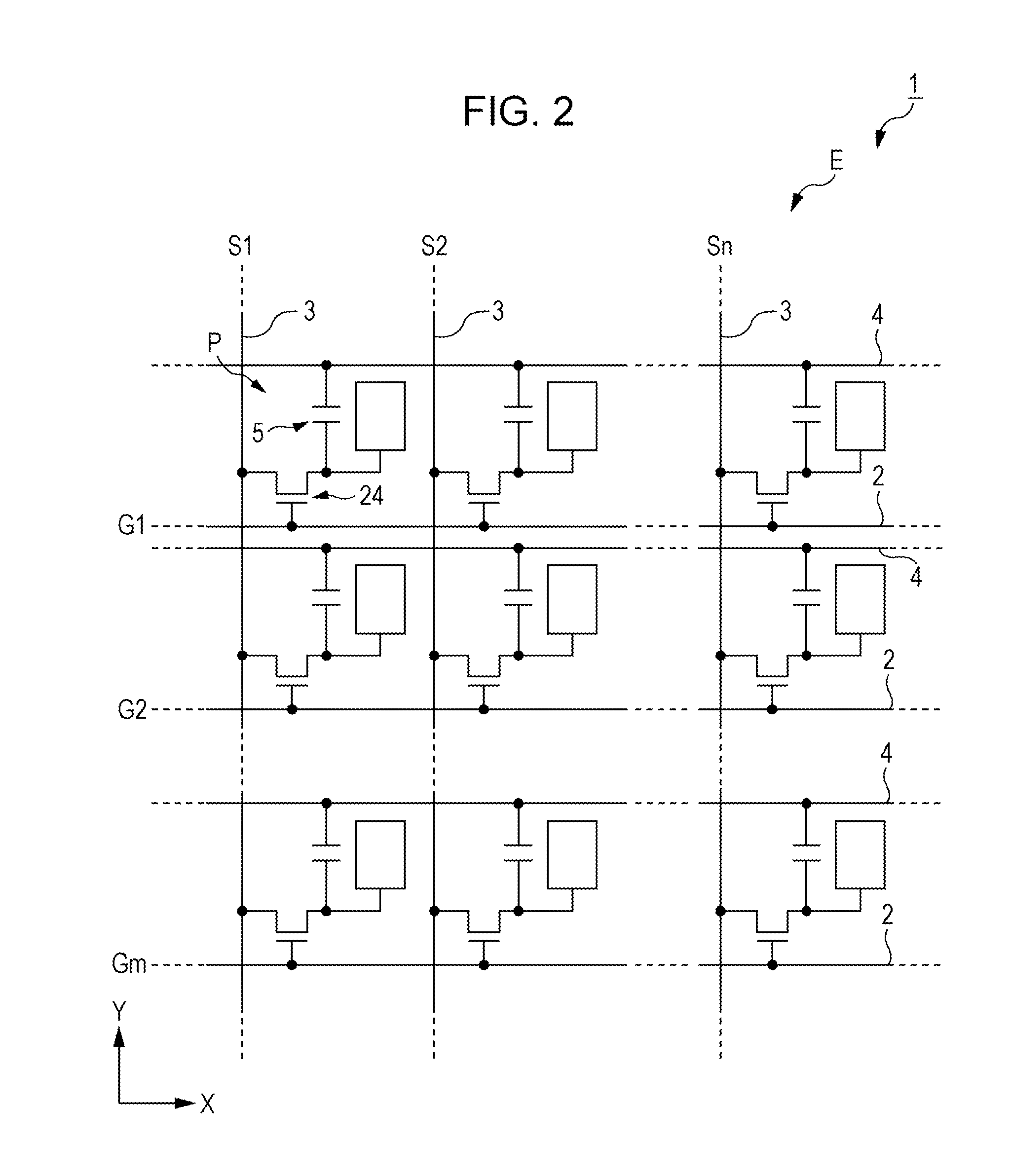
[0046]FIG. 1 is a schematic plan view showing a configuration of a liquid crystal device according to Embodiment 1. FIG. 2 is an equivalent circuit diagram showing an electrical configuration of the liquid crystal device according to Embodiment 1. FIG. 3 is a schematic cross-sectional view showing the configuration of the liquid crystal device according to Embodiment 1, and more specifically a partial schematic cross-sectional view taken along line A-A′ in FIG. 1 and along line B-B′ in FIG. 4. Firstly, a liquid crystal device 1 according to Embodiment 1 will be described with reference to FIGS. 1, 2, and 3.

[00...

modification example 1

Form with Locally Broken Symmetry

[0105]FIG. 9 is a diagram describing an example of the cell of microlens array according to Modification Example 1. Next, the microlens array 10 according to Modification Example 1 will be described with reference to FIG. 9. The same constituent parts as Embodiment 1 are given the same reference symbols and overlapping description will not be made.

[0106]The microlens array 10 of the modification example shown in FIG. 9, the shapes of the microlenses ML that configure the cell CL are different. Otherwise, the configuration is the same as Embodiment 1. In Embodiment 1 shown in FIG. 5B, although the symmetry of the microlens ML shapes in the cell CL is completely broken, and the microlens peaks MLP are disorderly arranged, the symmetry of the shapes of the microlenses ML may be partially broken, as shown in the modification example. For example, as shown in FIG. 9, diffraction caused by regularity of the microlenses ML is suppressed, even if the symmetr...

modification example 2

Form with Different Virtual Lattice Points

[0107]FIG. 10 is a diagram describing an example of a cell of a microlens array according to Modification Example 2. Next, the microlens array 10 according to Modification Example 2 will be described with reference to FIG. 10. The same constituent parts as Embodiment 1 are given the same reference symbols and overlapping description will not be made.

[0108]In the microlens array 10 of the modification example shown in FIG. 10, the virtual lattice points VLP of the microlenses ML that configure the cell CL are different. Otherwise, the configuration is the same as Embodiment 1. In Embodiment 1 shown in FIG. 5B, the virtual lattice point VLP is provided at the intersection point at which the cells CL are evenly divided. The virtual lattice point VLP is not limited thereto, and any arrangement may be used, if it has any symmetry. In FIG. 10, the virtual lattice points VLP are gathered in the center of the cell CL, and have translational symmetry...


PUM


Abstract

A microlens array includes a cell, and P lenses (P is an integer of 4 or more) arranged in the cell, in which the apexes of the P lenses are arranged such that symmetry is at least partially broken, when viewed in plan view. In this way, it is possible to suppress diffraction caused by regularity in the lens shape in the cell. Accordingly, it is possible to realize a microlens with a high utilization efficiency of light.

Description

BACKGROUND[0001]1. Technical Field[0002]The present invention relates to a microlens array, a method for manufacturing a microlens array, an electro-optical device, and an electronic apparatus.[0003]2. Related Art[0004]An electro-optical device is known which includes an electro-optical material, such as, a liquid crystal or the like, between an element substrate and a counter substrate. Examples of the electro-optical device include, for example, a liquid crystal device used as a liquid crystal light valve of a projector. There is demand for realizing a high optical utilization efficiency in such a liquid crystal device.[0005]A liquid crystal device is provided with TFT elements that drive pixels, wirings and the like outside a pixel region on an element substrate, and a light blocking layer is provided so as to planarly overlap thereupon. Therefore, a portion of the incident light is blocked by the light blocking layer and not utilized. A configuration is known in which incident l...

Claims


Application Information

Patent Timeline
IPC IPC(8): G02B3/00G02F1/1335
CPCG02B3/0056G02F1/133526G02B3/0025G02B3/0043G02B3/0006G02B3/0012G02B27/149G03B13/24G03B21/006G03B21/28H01L27/14603H01L27/14627
Inventor NIMURA, TORU
Owner SEIKO EPSON CORP
Why Eureka
Try Eureka