Negative characteristic thermistor and manufacturing method therefor
- Summary
- Abstract
- Description
- Claims
- Application Information
AI Technical Summary
Benefits of technology
Problems solved by technology
Method used
Image

Examples
embodiment 1
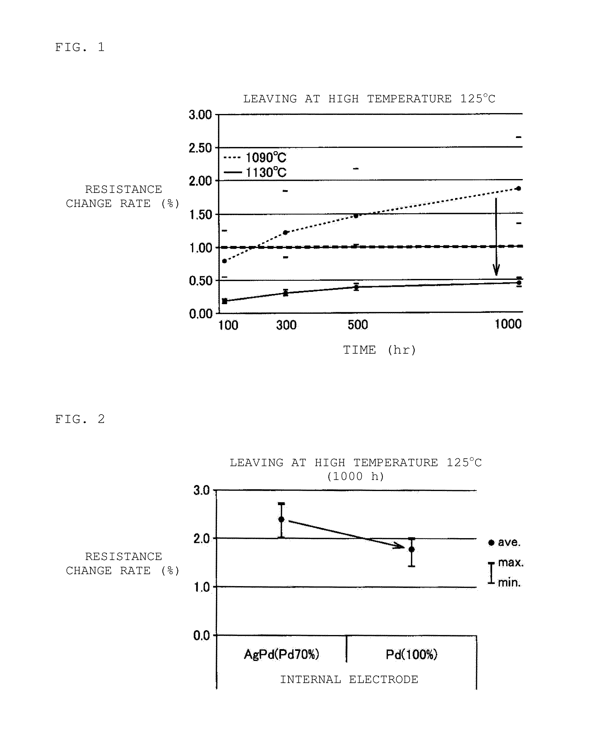
[0030]The laminated chip-type negative characteristic thermistor according to the present embodiment is a laminated chip-type negative characteristic thermistor including a ceramic element of a ceramic material containing Mn and Ni as its main constituents and containing Ti, and internal electrodes containing Pd ratio of 70 weight % or more, and having a size of 0603 size or less. The basic configuration is similar to a common configuration as described in, for example, Japanese Patent Application Laid-Open No. 2004-104093, the entire contents of which are incorporated herein by reference and the detailed descriptions of the configuration will be thus omitted.
[0031]The 0603 size herein refers to a size of 0.6 mm in a longer direction, 0.3 mm in a shorter direction, and 0.3 mm in a height direction. Further, the 1005 size refers to a size of 1.0 mm in a longer direction, 0.5 mm in a shorter direction, and 0.5 mm in a height direction.
[0032]The ceramic material constituting the cerami...
embodiment 2
[0038]The present embodiment differs from Embodiment 1 in that the size of the laminated chip-type negative characteristic thermistor is the 0402 size or less, with the use of internal electrodes of Pd, but provides, in the other respects, the same thermistor as in Embodiment 1. The other respects are similar to a common configuration as described in, for example, Japanese Patent Application Laid-Open No. 2004-104093, the entire contents of which are incorporated herein by reference and the detailed descriptions of the configuration will be thus omitted.
[0039]The 0402 size herein refers to a size of 0.4 mm in a longer direction, 0.2 mm in a shorter direction, and 0.2 mm in a height direction.
[0040]In the present embodiment, the ceramic element is preferably 16 μm or less in thickness. This is because the ceramic element has a thickness on the order of 16 μm, when the size of the laminated chip-type negative characteristic thermistor is the 0402 size or less.
embodiment 3
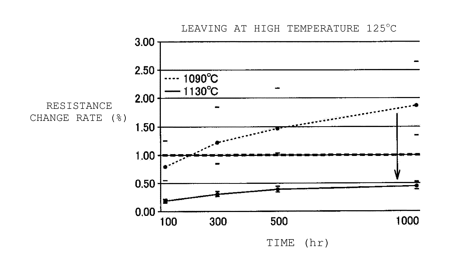
[0041]The present embodiment provides a method for manufacturing the laminated chip-type negative characteristic thermistor described in Embodiment 1 or 2, the method including a firing step at a temperature of 1100° C. or higher. The temperature of 1100° C. or higher in the firing step can densify the fired ceramic element.
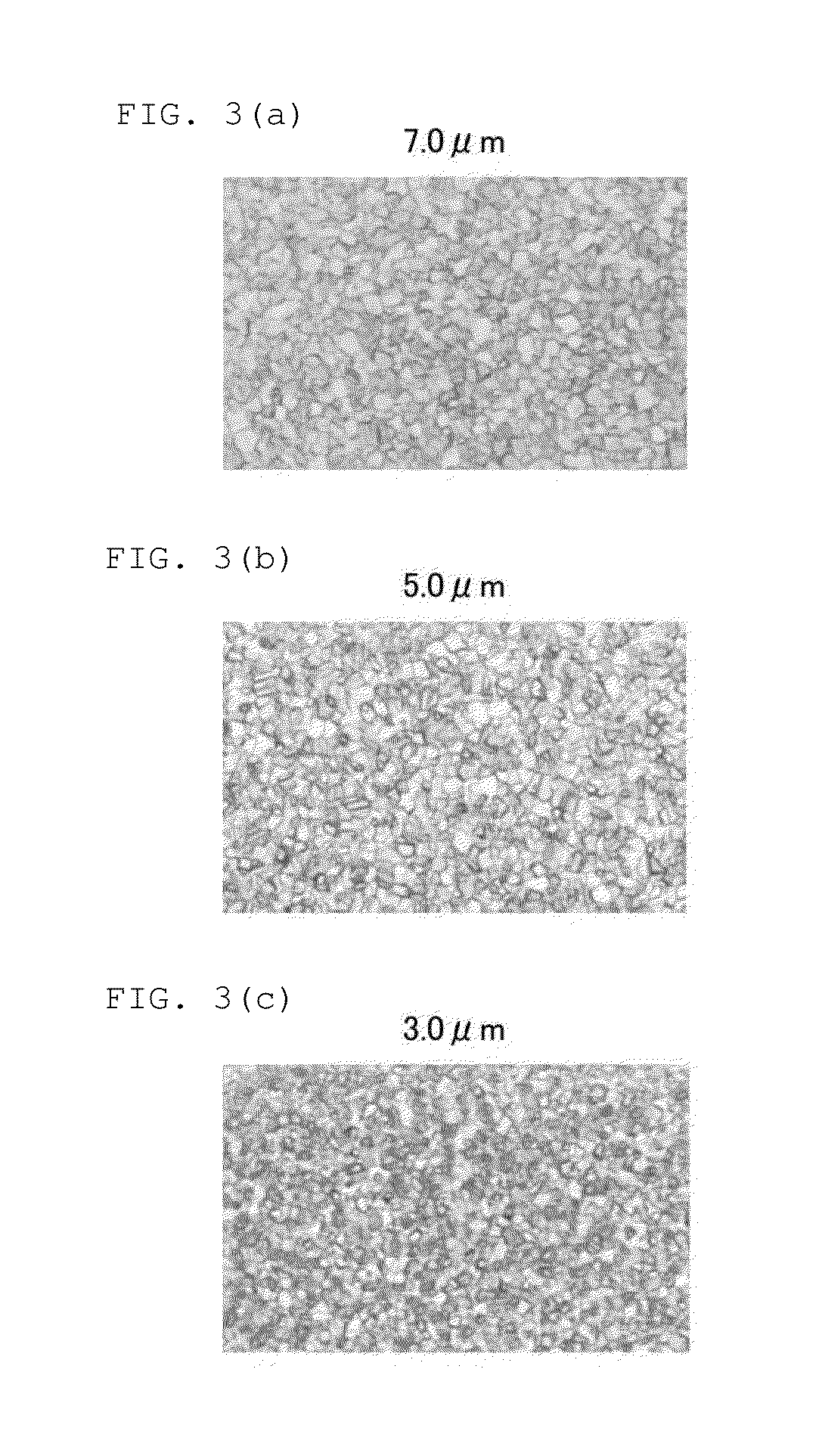
[0042]It is to be noted that the average grain size for the ceramic crystals of the fired ceramic element is preferably adjusted to 3.0 μm or less, and methods for the adjustment include, for example, a method of reducing particle sizes of a raw material powder for the ceramic element, and optimizing the amount of an organic binder in ceramic green sheets.
[0043]The manufacturing method according to the present embodiment can provide even laminated chip-type negative characteristic thermistors of 0603 size and 0402 size or less with an equivalent level of reliability to that of a large-size thermistor of 1005 size or more.
PUM
| Property | Measurement | Unit |
|---|---|---|
| Temperature | aaaaa | aaaaa |
| Thickness | aaaaa | aaaaa |
| Thickness | aaaaa | aaaaa |
Abstract
Description
Claims
Application Information
 - R&D Engineer
- R&D Manager
- IP Professional
- Industry Leading Data Capabilities
- Powerful AI technology
- Patent DNA Extraction
Browse by: Latest US Patents, China's latest patents, Technical Efficacy Thesaurus, Application Domain, Technology Topic.
© 2024 PatSnap. All rights reserved.Legal|Privacy policy|Modern Slavery Act Transparency Statement|Sitemap