Check patentability & draft patents in minutes with Patsnap Eureka AI!

Mechanical Compression-Based Method for the Reduction of Defects in Semiconductors

a mechanical compression and semiconductor technology, applied in the field of semiconductor defects, can solve the problems of deteriorating the reliability, efficiencies and lifetime of semiconductor devices, adding cost, time, and complexity of these processes, and achieve the effect of reducing defects

Inactive Publication Date: 2015-07-23
SANDIA
View PDF4 Cites 0 Cited by
  • Summary
  • Abstract
  • Description
  • Claims
  • Application Information

AI Technical Summary

Benefits of technology

The method described in this patent text offers a new way to make things like semiconductor materials and other materials that need defect removal. It uses a process that mimics embossing and imprinting to create large-scale fabrication and reduce defects.

Problems solved by technology

However, intrinsic defects such as stacking faults, threading dislocations, and point defects can seriously deteriorate semiconductor device reliability, efficiencies, and lifetimes. Therefore, strategies for the reduction of defects are of immense technological importance.
However, the added cost, time, and complexity of these processes are undesirable.

Method used


Image

  • Mechanical Compression-Based Method for the Reduction of Defects in Semiconductors
  • Mechanical Compression-Based Method for the Reduction of Defects in Semiconductors
  • Mechanical Compression-Based Method for the Reduction of Defects in Semiconductors

Examples


Embodiment Construction

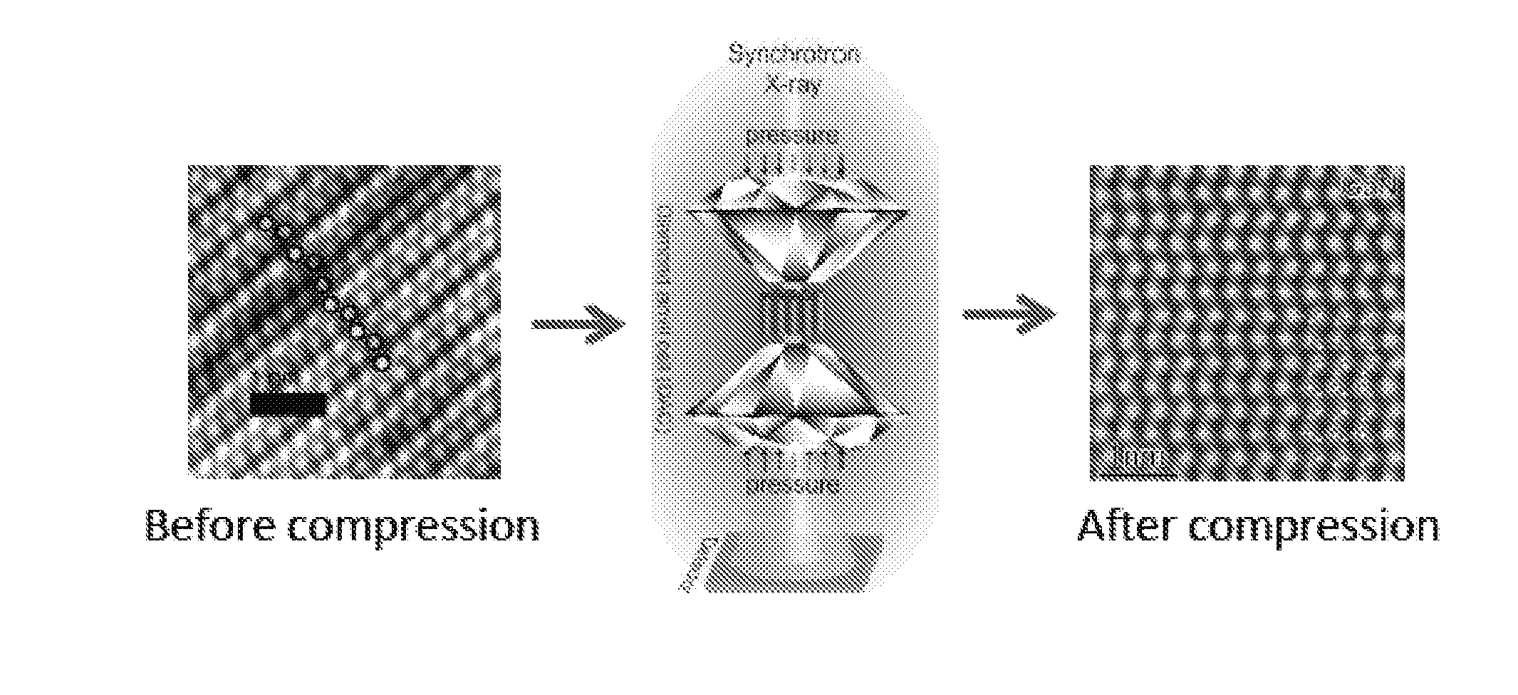
[0017]The discovery and understanding of high-pressure engineering processes has generated new scientific research and advanced scientific knowledge in defect reduction and the formation of new metal, semiconducting, and magnetic nanostructures that cannot be fabricated using conventional methods. Given that the low-pressure devices are readily and commercially available, the overall complexity and cost for defect reduction of epitaxial semiconductors can be drastically reduced with increased throughput using mechanical-compression based methods. The mechanical-compression method is a significant departure from current defect mitigation techniques, which rely on complex defect blocking masks, high temperature annealing, or re-crystallization that may be incompatible with the material or device. See S. D. Hersee et al., IEEE J. Quantum Electron. 38, 1017 (2002); Lei Li et al., Appl. Phys. Express 5 (2012); and J. C. Zolper et al., Appl. Phys. Lett. 68, 200 (1996). As an example of th...


PUM


Abstract

A high pressure-directed engineering method enables reduced defect semiconductor materials that are unattainable by other chemical and physical methods. Experimental results show that hydraulic pressures as low as 0.5 GPa can eliminate stacking faults and significantly reduce point defects, leading to improved materials quality in semiconductors, such as GaN.

Description

CROSS-REFERENCE TO RELATED APPLICATION[0001]This application claims the benefit of U.S. Provisional Application No. 61 / 928,517, filed Jan. 17, 2014, which is incorporated herein by reference.STATEMENT OF GOVERNMENT INTEREST[0002]This invention was made with Government support under contract no. DE-AC04-94AL85000 awarded by the U.S. Department of Energy to Sandia Corporation. The Government has certain rights in the invention.FIELD OF THE INVENTION[0003]The present invention relates to defects in semiconductors and, in particular, to a mechanical compression-based method for the reduction of defects in semiconductors.BACKGROUND OF THE INVENTION[0004]High quality semiconductor materials with low defect densities, such as III-nitride semiconductors, lead to more efficient, reliable UV to visible light-emitting diodes (LEDs), lasers, radiation detector, and RF devices with obvious impact in electronics, communications and surveillance. However, intrinsic defects such as stacking faults,...

Claims


Application Information

Patent Timeline
Patent Type & Authority Applications(United States)
IPC IPC(8): H01L21/322H01L21/46
CPCH01L21/46H01L21/322H01L21/02603H01L21/0242H01L21/02433H01L21/0254H01L21/02639H01L21/02653H01L21/02664H01L33/007H01L33/18H01L29/0669H01L29/2003H01L21/304
Inventor LI, QIMINGFAN, HONGYOU
Owner SANDIA
Features
  • R&D
  • Intellectual Property
  • Life Sciences
  • Materials
  • Tech Scout
  • Unparalleled Data Quality
  • Higher Quality Content
  • 60% Fewer Hallucinations
Learn More