Display device and method for driving the same

Active Publication Date: 2015-07-30
SHARP KK
View PDF7 Cites 69 Cited by
  • Summary
  • Abstract
  • Description
  • Claims
  • Application Information

AI Technical Summary

Benefits of technology

[0044]According to the first aspect of the present invention, in the second period, the predetermined number of scanning lines are sequentially selected and the drive current is measured with respect to each data line, thereby to acquire the first measurement data and the second measurement data with respect to each pixel circuit. Then, the video data is corrected based on the acquired first measurement data and second measurement data (hereinafter simply referred to as “measurement data” in the case of not distinguishing these in describing the effects of the invention). When the drive transistor is controlled in accordance with the data voltage based on the video data corresponding to the relatively low first gradation, the control voltage (gate-source voltage) of the drive transistor is relatively small, and hence a discrepancy of the threshold voltage with respect to the control voltage is greatly reflected to the drive current. In contrast, when the drive transistor is controlled in accordance with the data voltage based on the video data corresponding to the relatively high second gradation, the control voltage of the drive transistor is relatively large, and hence a discrepancy of the threshold voltage with respect to the control voltage is hardly reflected to the drive current, while a discrepancy of the gain is relatively greatly reflected to the drive current. For this reason, the first measurement data is data to which the discrepancy of the threshold voltage has been greatly reflected, and the second measurement data is data to which the discrepancy of the gain has been greatly reflected. In such a manner as above, the video data is corrected based on the first measurement data to which the discrepancy of the threshold voltage has been greatly reflected and the second measurement data to which the discrepancy of the gain has been greatly reflected, whereby it is possible to perform the threshold voltage compensation and the gain compensation of the drive transistor with respect to each pixel circuit. Further, since there is no need for stopping light emission of the electro-optic element except in a pixel circuit as a measurement target of the drive current in the second period, it is possible to perform the compensation while performing display. Moreover, since the video data is corrected based on the first measurement data and the second measurement data acquired in the second period, it is possible to perform the compensation following a change in characteristics of the drive transistor with time.
[0045]According to the second aspect of the present invention, the storage portion that stores the correction data is provided, and the correction data is updated based on the comparison results between the ideal characteristic data and the measurement data. By performing such an update of the correction data, it is possible to reliably perform the compensation following a change in cha

Problems solved by technology

An organic EL display device that employs the passive matrix system (hereinafter referred to as “passive matrix-type organic EL display

Method used


Image

  • Display device and method for driving the same
  • Display device and method for driving the same
  • Display device and method for driving the same

Examples


first embodiment

1. First Embodiment

1.1 Whole Configuration

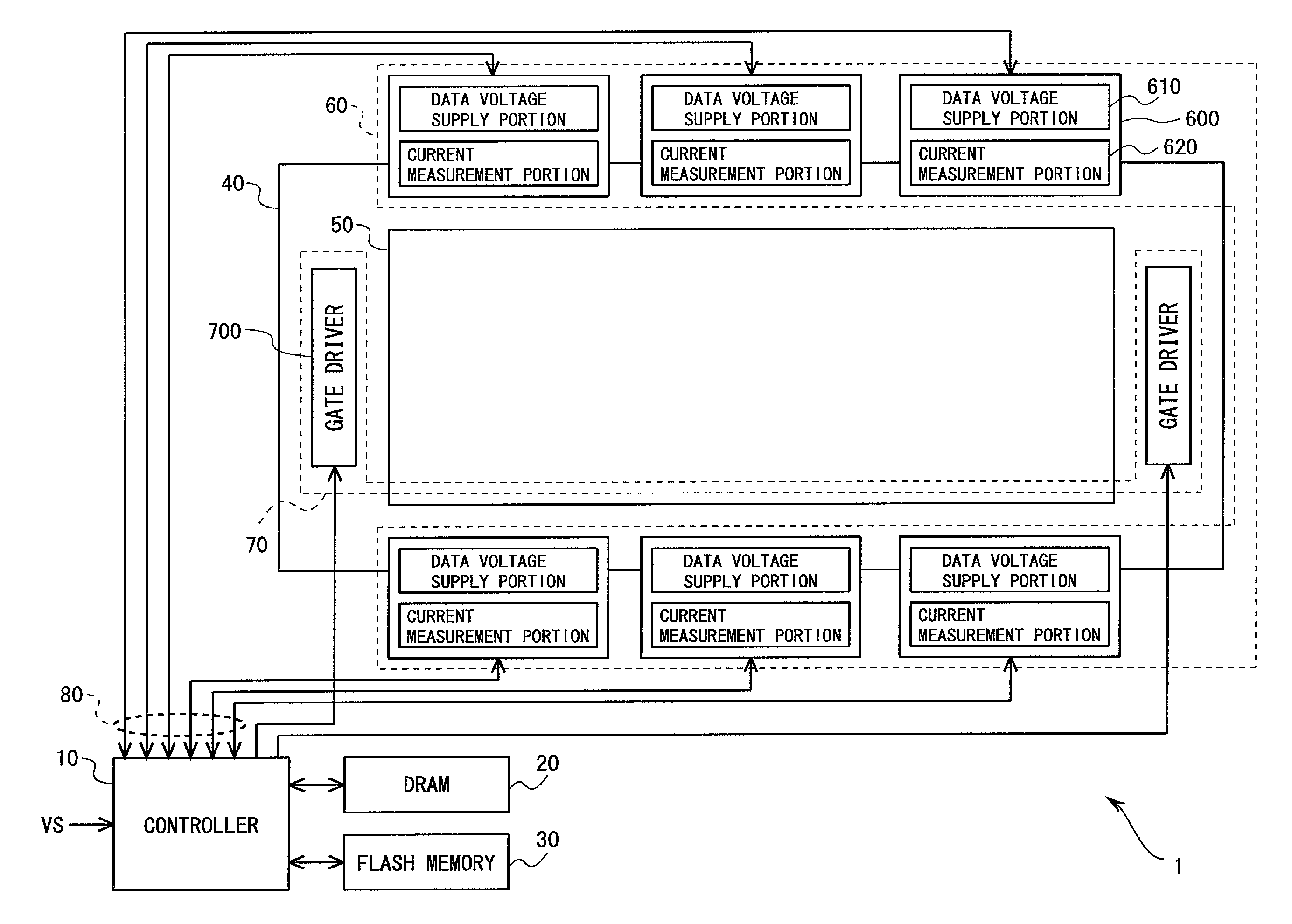
[0128]FIG. 1 is a block diagram showing a configuration of an active matrix-type organic EL display device 1 according to a first embodiment of the present invention. The organic EL display device 1 is provided with a controller 10, a DRAM (Dynamic Random Access Memory) 20, a flash memory 30, a display panel 40, a data drive portion 60, and a scanning drive portion 70. In the present embodiment, the controller 10 corresponds to the display control portion, and the DRAM 20 corresponds to the storage portion. A display portion 50 is formed in the display panel 40, and a data drive portion 60 and a scanning drive portion 70 are arranged on the display panel 40. It is to be noted that either the data drive portion 60 or the scanning drive portion 70 or both of them may be formed integrally with the display portion 50. Further, the DRAM and the flash memory 30 may be provided inside the controller 10.

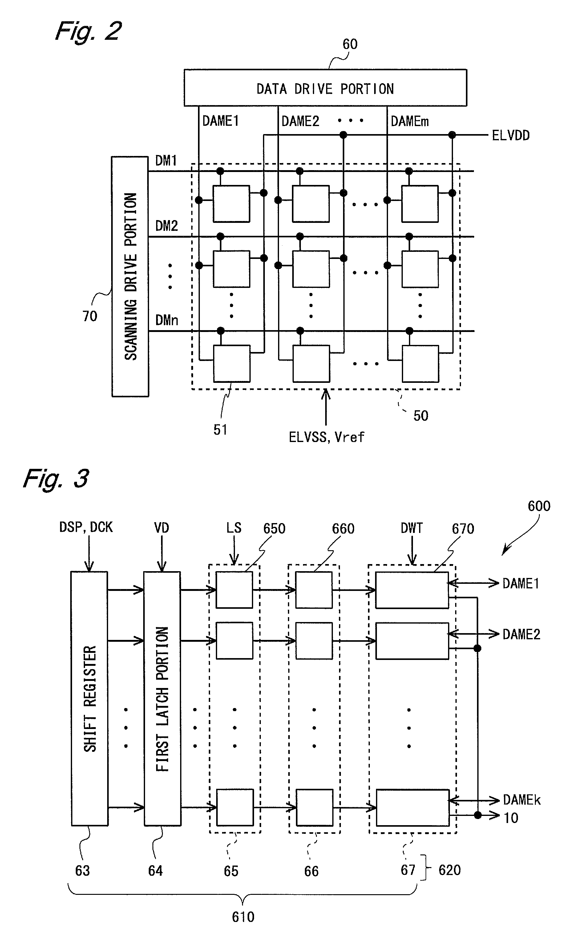
[0129]FIG. 2 is a block diagram for explaining...

second embodiment

2. Second Embodiment

[0260]

[0261]FIG. 37 is a circuit diagram showing a constitutional example of a data driver 600 in a second embodiment of the present invention. Out of the constitutional elements of the present embodiment, the same elements as those in the above first embodiment are provided with the same reference numerals, to omit descriptions thereof as appropriate. It is to be noted that in FIG. 37, only the constitutional elements on the i-th column and (i+1)-th column are shown (however, later-mentioned first and second selectors 760, 770, buffer amplifier 780 and measurement data acquirement portion 740 are constitutional elements in common between the plurality of columns). In a description of the present embodiment, as for symbols of the constitutional elements corresponding to the i-th column and the (i+1)-th column, “_i” and “_i+1” are added to the ends of those, respectively. It should be noted that hereinafter, the constitutional elements on the i-th column are mainl...

third embodiment

3. Third Embodiment

[0283]

[0284]FIG. 39 is a block diagram for explaining data communication between the controller 10 and the data driver 600 in a third embodiment of the present invention. Out of the constitutional elements of the present embodiment, the same elements as those in the above first embodiment are provided with the same reference numerals, to omit descriptions thereof as appropriate. A communication bus in the present embodiment is configured of a bidirectional communication bus capable of performing bidirectional data communication between the controller 10 and the data driver 600. In addition, the kind of bidirectional communication bus is not particularly restricted, but it is an LVDS, an MIPI, an e-DP or the like, for example.

[0285]

[0286]FIG. 40 is a timing chart for explaining timing for receiving video data and sending measurement data in a vertical synchronization period of an N-th frame period in the present embodiment. In the present embodiment, assuming p=7, ...


PUM


Abstract

An organic EL display device includes a controller, a data driver, and a DRAM which provides a gain correction memory and a threshold voltage correction memory. The data driver sends, to the controller, first and second measurement data Im corresponding to the first and second measuring data voltages Vm, respectively. The controller compares ideal characteristic data IO(P) with the first and second measurement data Im, and updates threshold voltage correction data Vt and gain correction data B2R based on the comparison results. The controller corrects video data Vm based on the threshold voltage correction data Vt and the gain correction data B2R. Thereby, both threshold voltage compensation and gain compensation of a drive transistor are performed with respect to each pixel circuit, while display is performed.

Description

TECHNICAL FIELD[0001]The present invention relates to a display device, and more specifically relates to a display device provided with a pixel circuit including an electro-optic element such as an organic EL (Electro Luminescence) element, and a method for driving the same.BACKGROUND ART[0002]As a display element provided in a display device, there have hitherto been an electro-optic element whose luminance is controlled by an applied voltage, and an electro-optic element whose luminance is controlled by a flowing current. Examples of the electro-optic element whose luminance is controlled by an applied voltage include a liquid crystal display element. Meanwhile, examples of the electro-optic element whose luminance is controlled by a flowing current include an organic EL element. The organic EL display device using the organic EL element as a self-emitting element can be reduced in thickness and power consumption and increased in luminance as compared to the liquid crystal display...

Claims


Application Information

Patent Timeline
IPC IPC(8): G09G3/32
CPCG09G3/3233G09G2300/0852G09G2310/027G09G2310/0286G09G2310/0291G09G2310/0294G09G2320/043G09G3/3266G09G3/3291G09G2300/0842G09G2300/0861G09G2320/0233G09G2320/029G09G2320/0295H10K59/131
Inventor TAKAHAMA, KENGOYAMAUCHI, YOSHIMITSUNOGUCHI, NOBORUKISHI, NORITAKA
Owner SHARP KK
Why Eureka
Try Eureka