Photoconductive antenna, camera, imaging device, and measurement device

a technology of photoconductive antennas and imaging devices, applied in the field of photoconductive antennas, can solve the problems of not being able to generate terahertz waves having a large intensity, not being able to realize cameras, imaging devices, and measurement devices with high detection sensitivity, and achieve the effect of high detection sensitivity

Inactive Publication Date: 2015-07-30
SEIKO EPSON CORP
View PDF7 Cites 4 Cited by
  • Summary
  • Abstract
  • Description
  • Claims
  • Application Information

AI Technical Summary

Benefits of technology

[0035]In such a measurement device, since the photoconductive antenna according to

Problems solved by technology

In the photoconductive antenna disclosed in JP-A-2009-124437, since the carrier mobility (electron mobility) of the LT-GaAs layer has a small rate of 100 cm2/Vs to 150 cm2/Vs, the time variation of a photocurrent decreases, an

Method used


Image

  • Photoconductive antenna, camera, imaging device, and measurement device
  • Photoconductive antenna, camera, imaging device, and measurement device
  • Photoconductive antenna, camera, imaging device, and measurement device

Examples


first modification example

3.1. First Modification Example

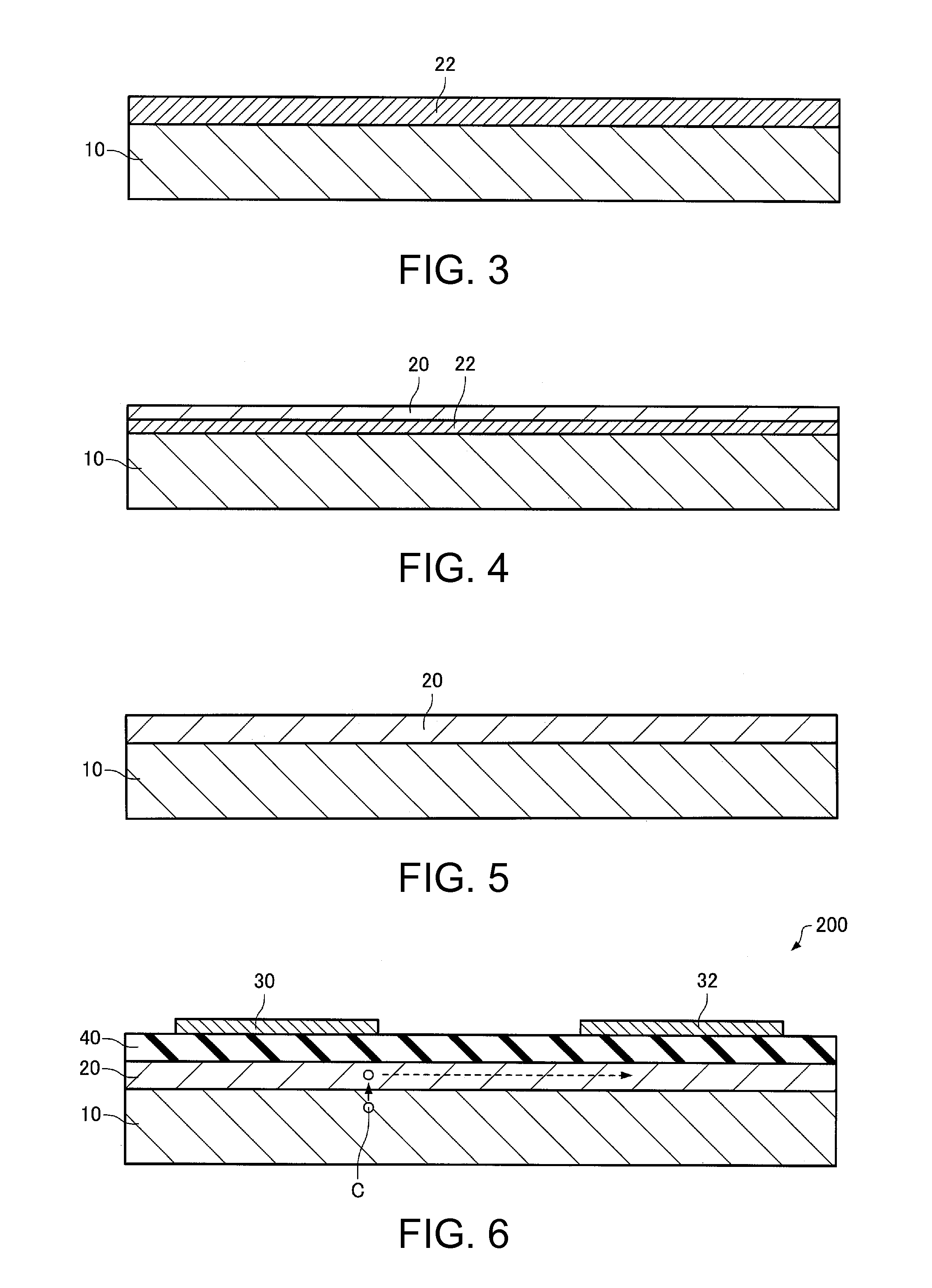
[0088]Next, a photoconductive antenna according to a first modification example of the present embodiment will be described with reference to the accompanying drawings. FIG. 6 is a cross-sectional view schematically illustrating a photoconductive antenna 200 according to the first modification example of the present embodiment, and corresponds to FIG. 1.

[0089]Hereinafter, in the photoconductive antenna 200 according to the first modification example of the present embodiment, members having the same functions as the configuration members of the aforementioned photoconductive antenna 100 according to the present embodiment are assigned the same reference numerals and signs, and thus the detailed description thereof will be omitted. The same is true of a photoconductive antenna according to a second modification example of the present embodiment described below.

[0090]As shown in FIG. 6, the photoconductive antenna 200 is different from the aforementioned...

second modification example

3.2. Second Modification Example

[0094]Next, a photoconductive antenna according to a second modification example of the present embodiment will be described with reference to the accompanying drawings. FIG. 7 is a cross-sectional view schematically illustrating a photoconductive antenna 300 according to the second modification example of the present embodiment, and corresponds to FIG. 1.

[0095]As shown in FIG. 7, the photoconductive antenna 300 is different from the aforementioned photoconductive antenna 100, in that a third layer 50 is included therein.

[0096]The third layer 50 is located on the first layer 10. The third layer 50 is located between the first layer 10 and the second layer 20. Openings 52 are provided in the third layer 50. In the shown example, two opening 52 are provided, but the number thereof is not particularly limited. The openings 52 are filled with the second layer 20. The carriers C generated in the first layer 10 pass through, for example, the openings 52, an...


PUM


Abstract

A photoconductive antenna that generates a terahertz wave by irradiation with a light pulse, includes: a first layer that has carriers formed therein by irradiation with the light pulse; a second layer, located above the first layer, which has carrier mobility larger than carrier mobility of the first layer; and a first electrode and a second electrode, located above the second layer, which apply a voltage to the second layer.

Description

BACKGROUND[0001]1. Technical Field[0002]The present invention relates to a photoconductive antenna, a camera, an imaging device, and a measurement device.[0003]2. Related Art[0004]In recent years, terahertz waves which are electromagnetic waves having a frequency equal to or greater than 100 GHz and equal to or less than 30 THz have attracted attention. The terahertz waves can be used in, for example, various types of measurement such as imaging and spectroscopic measurement, non-destructive tests, and the like.[0005]Terahertz wave generation devices that generate such terahertz waves include, for example, a light pulse generation device that generates a light pulse having a pulse width of approximately subpicoseconds (several hundred femtoseconds), and a photoconductive antenna that generates a terahertz wave by irradiation with the light pulse generated in the light pulse generation device.[0006]For example, JP-A-2009-124437 discloses a photoconductive antenna including a semi-ins...

Claims


Application Information

Patent Timeline
IPC IPC(8): H01L31/16G01N21/3581
CPCH01L31/16G01N2201/0696G01N2201/061G01N21/3581
Inventor TAKENAKA, SATOSHI
Owner SEIKO EPSON CORP
Why Eureka
Try Eureka