Substrate processing apparatus, substrate transfer method and substrate transfer device

a technology of substrate and processing apparatus, applied in the direction of storage devices, manipulators, electrical apparatus, etc., can solve the problems of substrate damage, particle generation, and the inability to transfer substrate from a certain place to a certain other place, so as to prevent photo-corrosion and prevent photo-corrosion

Inactive Publication Date: 2015-08-06
EBARA CORP
View PDF2 Cites 1 Cited by
  • Summary
  • Abstract
  • Description
  • Claims
  • Application Information

AI Technical Summary

Benefits of technology

[0017]The present invention has been made in view of the above situation. It is therefore a first object of the present invention to provide a substrate processing apparatus which can prevent photo-corrosion of, e.g., copper interconnects due to exposure of a surface to be processed of a substrate to light and, even during maintenance work on a processing unit in the apparatus, can perform processing, such as cleaning, of a substrate surface while preventing photo-corrosion of, e.g., copper interconnects due to exposure to light, though the number of processable substrates decreases during the maintenance work.
[0018]It is a second object of the present invention to provide a substrate transfer method and a substrate transfer device which can broaden the acceptable range of positioning adjustment for a substrate transfer device and can prevent damage to a substrate, the generation of particles and a substrate transfer failure.
[0020]By thus using the processing units which have been subjected to light shielding processing, providing the light shielding wall between the transfer area and each of the two adjacent processing areas and providing the light-shielding maintenance door for the front opening of the transfer area, external light can be prevented from entering the transfer area even when a maintenance door for a processing unit is open.
[0024]When the shutter of a processing unit is open, a substrate can be transferred to or from the processing unit while keeping the interiors of the processing unit and the transfer area in a light-shielded environment. By closing the shutter of the processing unit, external light can be prevented from entering the transfer area through the opening of the light shielding wall, e.g., during maintenance work on the processing unit.
[0032]The substrate processing apparatus of the present invention can prevent photo-corrosion of, e.g., copper interconnects due to exposure of a surface to be processed of a substrate to light and, even during maintenance work on a processing unit in the apparatus, can perform processing, such as cleaning, of a substrate surface while preventing photo-corrosion of, e.g., copper interconnects due to exposure to light, though the number of processable substrates decreases temporarily during the maintenance work.
[0033]According to the substrate transfer method and the substrate transfer device of the present invention, the clearance permits lateral movement of a substrate when it is placed on a substrate support (e.g., a temporary holder), and therefore the substrate and the substrate support will not strongly rub together. This can prevent damage to the substrate, the generation of particles, and a failure in transfer of the substrate.

Problems solved by technology

When the maintenance door is opened, light will enter the apparatus and may cause photo-corrosion of, e.g., copper interconnects exposed on a surface (surface to be processed) of a substrate.
If the positioning adjustment is insufficient, it is possible that friction may occur between a substrate and the substrate support, causing damage to the substrate and generating particles.
Further, in some cases, a substrate cannot be transferred from a certain place to a certain other place.

Method used


Image

  • Substrate processing apparatus, substrate transfer method and substrate transfer device
  • Substrate processing apparatus, substrate transfer method and substrate transfer device
  • Substrate processing apparatus, substrate transfer method and substrate transfer device

Examples


Embodiment Construction

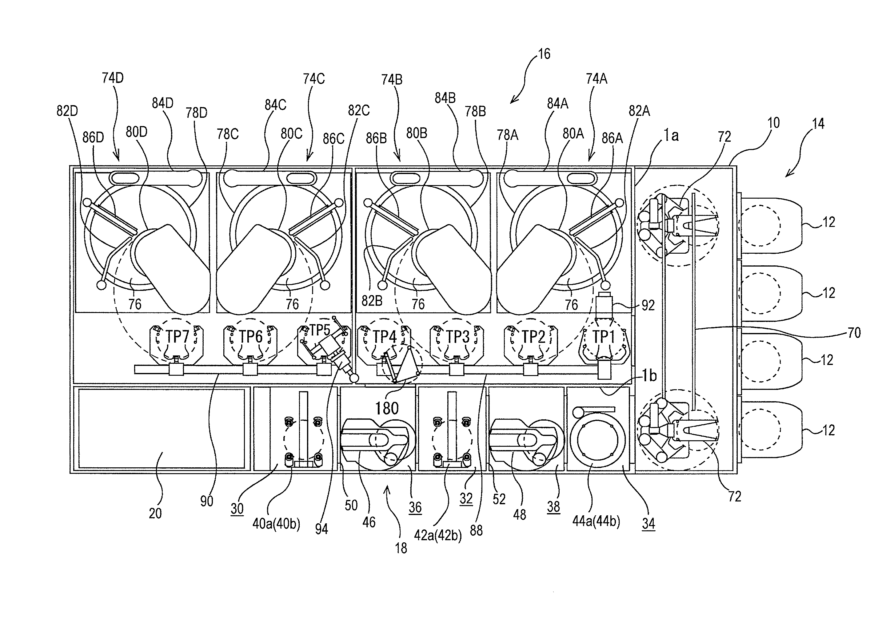
[0046]Preferred embodiments of the present invention will now be described in detail with reference to the drawings. The following description illustrates an exemplary case in which a substrate processing apparatus according to the present invention is applied to a cleaning section provided in a CMP (chemical mechanical polishing) apparatus which removes an unnecessary portion of a copper plated film formed on a surface of a substrate, such as a semiconductor wafer, i.e. a portion other than a copper plated film embedded in interconnect trenches and vias, thereby forming copper interconnects.

[0047]A substrate processing apparatus according to the present invention can, of course, be applied to a cleaning section of an apparatus different from a CMP apparatus or to a processing section different from a cleaning section if such a cleaning section or processing section is required to prevent photo-corrosion due to exposure to light.

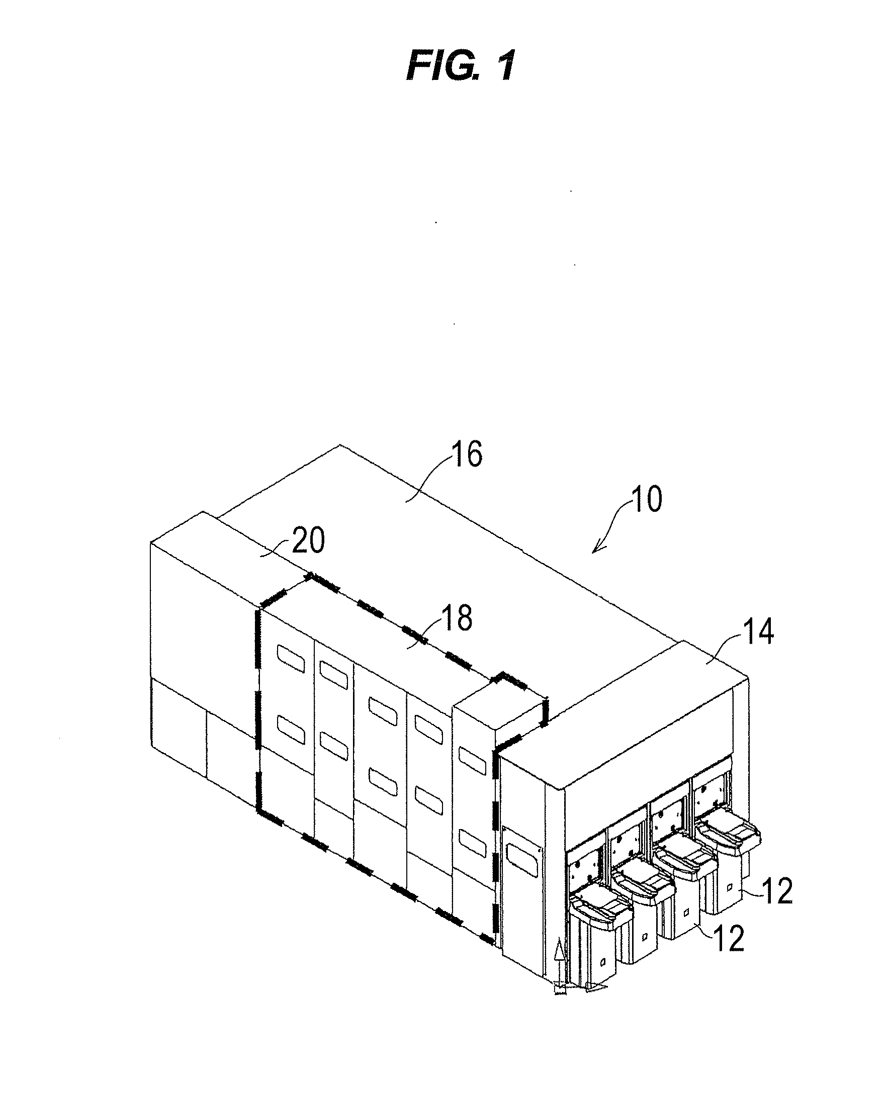
[0048]FIG. 1 shows an overall external view of a CMP a...


PUM


Abstract

A substrate processing apparatus can prevent photo-corrosion of, e.g., copper interconnects due to exposure of a surface to be processed of a substrate to light, and can perform processing, such as cleaning, of a substrate surface while preventing photo-corrosion of, e.g., copper interconnects due to exposure to light. The substrate processing apparatus includes a plurality of processing areas housing therein processing units which have been subjected to light shielding processing; and at least one transfer area housing therein a transfer robot and disposed between two adjacent ones of the plurality of processing areas. A light shielding wall is provided between the transfer area and each of the two adjacent processing areas, and a light-shielding maintenance door is provided for the front opening of the transfer area. The processing units are coupled to the light shielding walls in a light-shielding manner.

Description

CROSS-REFERENCE TO RELATED APPLICATIONS[0001]This document claims priorities to Japanese Application Number 2011-123369, filed Jun. 1, 2011 and Japanese Application Number 2011-173704, filed Aug. 9, 2011, the entire contents of which are hereby incorporated by reference.BACKGROUND OF THE INVENTION[0002]1. Field of the Invention[0003]The present invention relates to a substrate processing apparatus, and more particularly to a substrate processing apparatus which can perform processing, such as cleaning, of a surface (surface to be processed) of a substrate, such as a semiconductor wafer, while preventing photo-corrosion of, e.g., copper interconnects, formed in the surface of the substrate, due to exposure of the interconnects to light.[0004]The present invention also relates to a substrate transfer method for transferring a substrate and a substrate transfer device, and more particularly to a substrate transfer method for transferring a substrate in a substrate processing apparatus ...

Claims


Application Information

Patent Timeline
Patent Type & Authority Applications(United States)
IPC IPC(8): H01L21/677B25J11/00
CPCH01L21/6704H01L21/67173H01L21/67196H01L21/67219H01L21/67718H01L21/68707B25J11/0095H01L21/67706H01L21/67742
Inventor YOKOYAMA, TOSHIOKUNISAWA, JUNJIMIYAZAKI, MITSURUSUZUKI, KENICHISOTOZAKI, HIROSHI
Owner EBARA CORP
Why Eureka
Try Eureka