Drive device
a technology of drive device and clamp switch, which is applied in the direction of electric devices, pulse generators, pulse techniques, etc., can solve the problems of circuit elements malfunctioning and erroneous firing, and achieve the effect of reducing the influence of heat generation and/or wiring impedance on the clamp switch provided in the drive devi
- Summary
- Abstract
- Description
- Claims
- Application Information
AI Technical Summary
Benefits of technology
Problems solved by technology
Method used
Image

Examples
embodiment 1
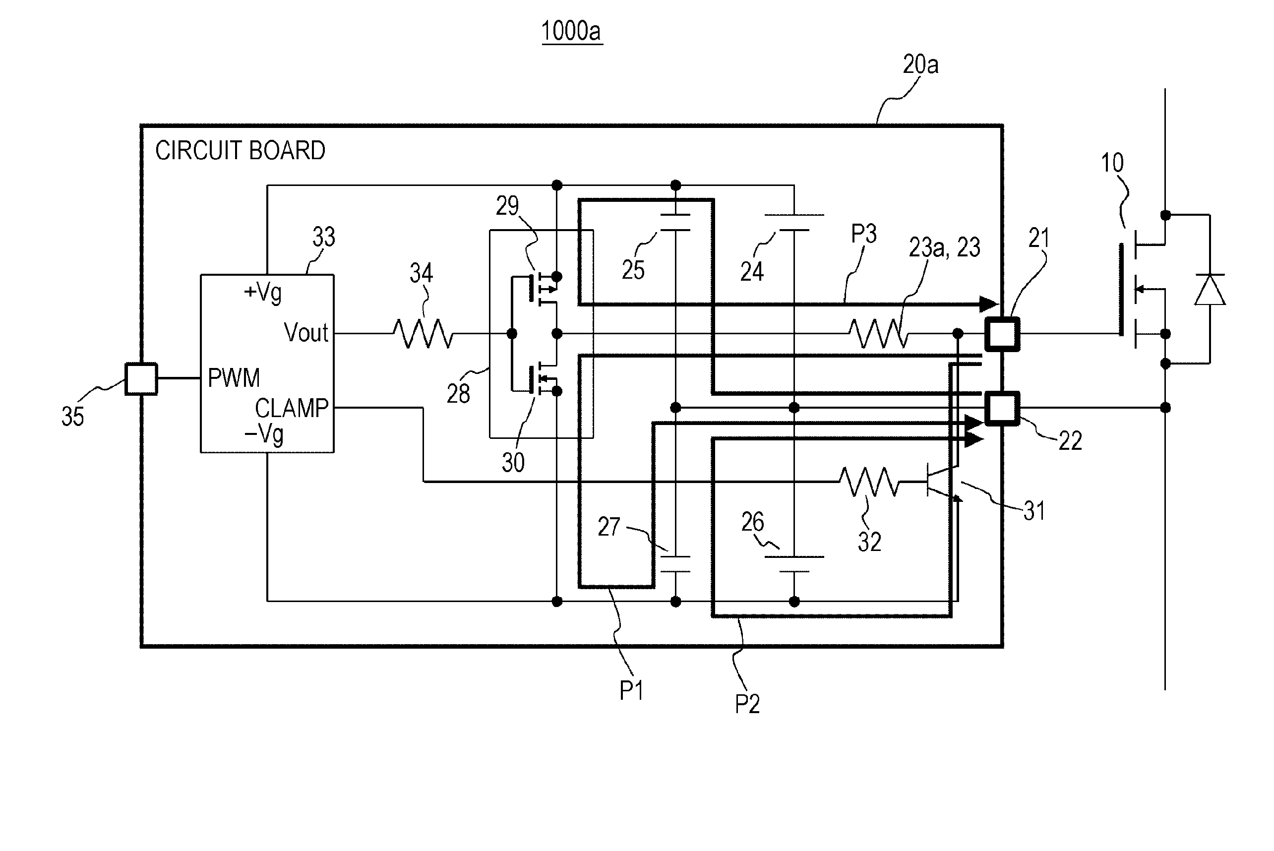
[0062]FIG. 1 is a diagram illustrating an example of a configuration of a gate drive circuit according to embodiment 1 of the disclosure. The gate drive circuit 1000a is a circuit for driving a power switch 10. The power switch 10 includes a control terminal, a first conduction terminal, and a second conduction terminal, for instance. The power switch 10 may be a gate insulating transistor, for instance. The gate insulating transistor may be MOSFET or IGBT that is made from Si, SiC, or GaN, for instance. On condition that the power switch 10 is MOSFET, the control terminal corresponds to a gate terminal, one of the first conduction terminal and the second conduction terminal corresponds to a source terminal, and the other corresponds to a drain terminal. On condition that the power switch 10 is IGBT, the control terminal corresponds to a gate terminal, one of the first conduction terminal and the second conduction terminal corresponds to an emitter terminal, and the other correspond...
embodiment 2
[0114]FIG. 5 is a diagram illustrating an example of a configuration of a gate drive circuit according to embodiment 2. The example of the configuration of the gate drive circuit 1000b which is illustrated in FIG. 5 includes the gate drive circuit 1000a which is illustrated in FIG. 1 and from which the negative bias power supply 26 and the negative bias capacitor 27 are removed. The gate drive circuit 1000b is capable of applying a positive bias voltage but incapable of applying a negative bias voltage between the gate and the source of the power switch 10, based on the potential at the source terminal of the power switch 10. For instance, on-voltage the gate drive circuit 1000b outputs is set at +Vg=20 V and off-voltage is set at 0 V.
[0115]The gate drive circuit 1000b does not include the negative bias capacitor 27. Therefore, synthetic impedance of a discharge path P1m in the gate drive circuit 1000b is smaller than the synthetic impedance of the discharge path P1 in the gate driv...
embodiment 3
[0118]FIG. 6 is a diagram illustrating an example of a configuration of a gate drive circuit according to embodiment 3. The gate drive circuit 1000c illustrated in FIG. 6 has basically the same configuration as the gate drive circuit 1000a illustrated in FIG. 1 has, except that the clamp switch 31 is depicted as a switch symbol instead of a transistor symbol. In addition, the clamp resistor 32 is omitted in depiction.
[0119]The gate drive circuit 1000c illustrated in FIG. 6 includes a current limit circuit 36 between the wiring line extending between the gate terminal connector 21 and the current limit circuit 23 and the control terminal of the clamp switch 31. The current limit circuit 36 is a circuit for preventing malfunction of the clamp switch 31. The current limit circuit 36 may be a resistor, for instance, or may be other elements such as capacitor. In case where the instantaneous current is generated at the control terminal of the clamp switch 31 when the clamp switch 31 is i...
PUM
 Abstract
Description
Claims
Application Information
 - R&D
- Intellectual Property
- Life Sciences
- Materials
- Tech Scout
- Unparalleled Data Quality
- Higher Quality Content
- 60% Fewer Hallucinations
Browse by: Latest US Patents, China's latest patents, Technical Efficacy Thesaurus, Application Domain, Technology Topic, Popular Technical Reports.
© 2025 PatSnap. All rights reserved.Legal|Privacy policy|Modern Slavery Act Transparency Statement|Sitemap|About US| Contact US: help@patsnap.com