High reliability semiconductor package structure

a semiconductor and high-reliability technology, applied in semiconductor devices, semiconductor/solid-state device details, electrical devices, etc., can solve reliability-related problems and short circuits of products, and achieve the effects of enhancing the reliability of semiconductor package structures, absorbing and dissipating transient high-power heat, and quick absorbing and dissipation

Active Publication Date: 2015-08-27
ANOVA TECH
View PDF3 Cites 13 Cited by
  • Summary
  • Abstract
  • Description
  • Claims
  • Application Information

AI Technical Summary

Benefits of technology

[0008]The present invention provides a high-reliability semiconductor package structure which comprises a lower heat sink, a die, an upper heat sink, a lead frame, and a package body. The upper heat sink and the lower heat sink are adhered tightly to two opposing surfaces of the die, respectively, to effectively absorb and dissipate transient high-power heat. The lower heat sink has a recess for surrounding the die to prevent a solder from overflowing and thus

Problems solved by technology

The lower heat sink has a recess for surrounding the die to prevent a solder from overflowi

Method used


Image

  • High reliability semiconductor package structure
  • High reliability semiconductor package structure
  • High reliability semiconductor package structure

Examples


Embodiment Construction

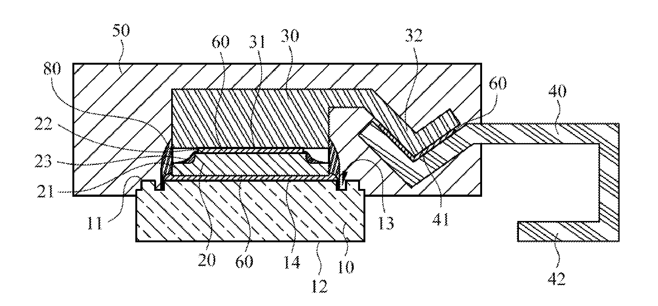
[0026]Referring to FIG. 3, in the embodiment of the present invention, a high-reliability semiconductor package structure 100 comprises a lower heat sink 10, a die 20, an upper heat sink 30, a lead frame 40 and a package body 50.

[0027]Referring to FIG. 3 and FIG. 4, the high-reliability semiconductor package structure 100 is manufactured to be a DO-218(AB) package structure or a TO-220 package structure, and is for use as a high power EMC protects component, a high power voltage regulation IC, a transient state voltage suppressing chip, or a Zener chip.

[0028]Referring to FIG. 3 and FIG. 4, the lower heat sink 10 is made of a thermally conductive material and has an upper surface 11 and a bottom surface 12. The upper surface 11 has an annular recess 13 which surrounds an adhesion region 14 of the upper surface 11. The lower heat sink 10 has a volume for absorbing a portion of the heat generated from the die 20 and dissipating the heat from its bottom. The recess 13 is U-shaped, V-sha...


PUM


Abstract

The present invention discloses a high reliability semiconductor package structure, which includes a lower heat sink, a die, an upper heat sink, a lead frame and a package body. The lead frame and the upper heat sink contain separately a first bending unit and a second bending unit that are electrically connected. The upper and lower heat sinks are attached to two opposite surfaces of the die and sink the high power transient heat generated at the die. The lower heat sink also has an indentation that circles the die and contains extra solder that might otherwise contaminate the die. Package body contains and protects the die, the upper and lower heat sinks and the lead frame. With the implementation of the invention, the reliability of the semiconductor package structure is promoted and the EMC durability together with the operable power is enhanced.

Description

[0001]This application claims priority to Taiwan Patent Application No. 103106596, filed on Feb. 26, 2014, which is hereby incorporated by reference.BACKGROUND OF THE INVENTION[0002]1. Technical Field[0003]The present invention relates to semiconductor package structures, and more particularly, to a high-reliability semiconductor package structure.[0004]2. Description of Related Art[0005]Due to technological advancement, vehicular electronic systems are being rapidly incorporated into various types of vehicles. For instance, intricate and precise electronic circuit systems, such as vehicular inductive radar, vehicular hi-fi, and various vehicular safety systems are widely incorporated into and applied to various types of vehicles. However, EMC-related problems and voltage regulation-related problems which arise inevitably from electronic circuit systems are becoming more serious. For the details of the challenges posed by EMC or voltage regulation to the vehicular electronic circuit...

Claims


Application Information

Patent Timeline
IPC IPC(8): H01L23/495H01L27/02H01L23/31H01L23/373H01L23/00H01L23/043H01L23/367
CPCH01L23/49544H01L23/49551H01L23/043H01L27/0248H01L23/3675H01L23/3736H01L2224/33181H01L23/3107H01L2924/01029H01L2924/1715H01L2924/12035H01L2224/32245H01L24/33H01L2924/181H01L23/3171H01L23/4334H01L23/49555H01L23/49568H01L23/49524H01L29/0657H01L2224/40095H01L2224/40245H01L24/40H01L2224/73263H01L2924/12036H01L2224/27013H01L2924/10155H01L2224/84385H01L2224/84801H01L2224/83801H01L2924/00014H01L2224/84345H01L24/29H01L24/32H01L24/37H01L2224/32013H01L2224/32112H01L2224/06181H01L2224/26175H01L2224/29023H01L2224/291H01L2224/32111H01L24/84H01L2924/00H01L2924/00012H01L2224/37099H01L2924/014H01L24/36
Inventor YANG, WEI-LICHOU, TSUNG-CHIEHWANG, I, TZU-CHIANGCHANG, TSANG-SHENG
Owner ANOVA TECH
Why Eureka
Try Eureka