Display device

Active Publication Date: 2015-08-27
SAMSUNG DISPLAY CO LTD
View PDF7 Cites 11 Cited by
  • Summary
  • Abstract
  • Description
  • Claims
  • Application Information

AI Technical Summary

Benefits of technology

[0021]According to embodiments of the present invention, the display device includes a pad area, configured to transmit drive power to first and second electrodes, on a sealing member so that a dead space of a first substrate decreases, and the drive power is directly supplied to a display area through the sealing member so that voltage drop is reduced, the drive power is u

Problems solved by technology

However, the above flat panel displays have an intricate structure, and as the number of chip on film (COF), flexible printed ci

Method used


Image

  • Display device
  • Display device
  • Display device

Examples


Example

First Embodiment of the Present Invention

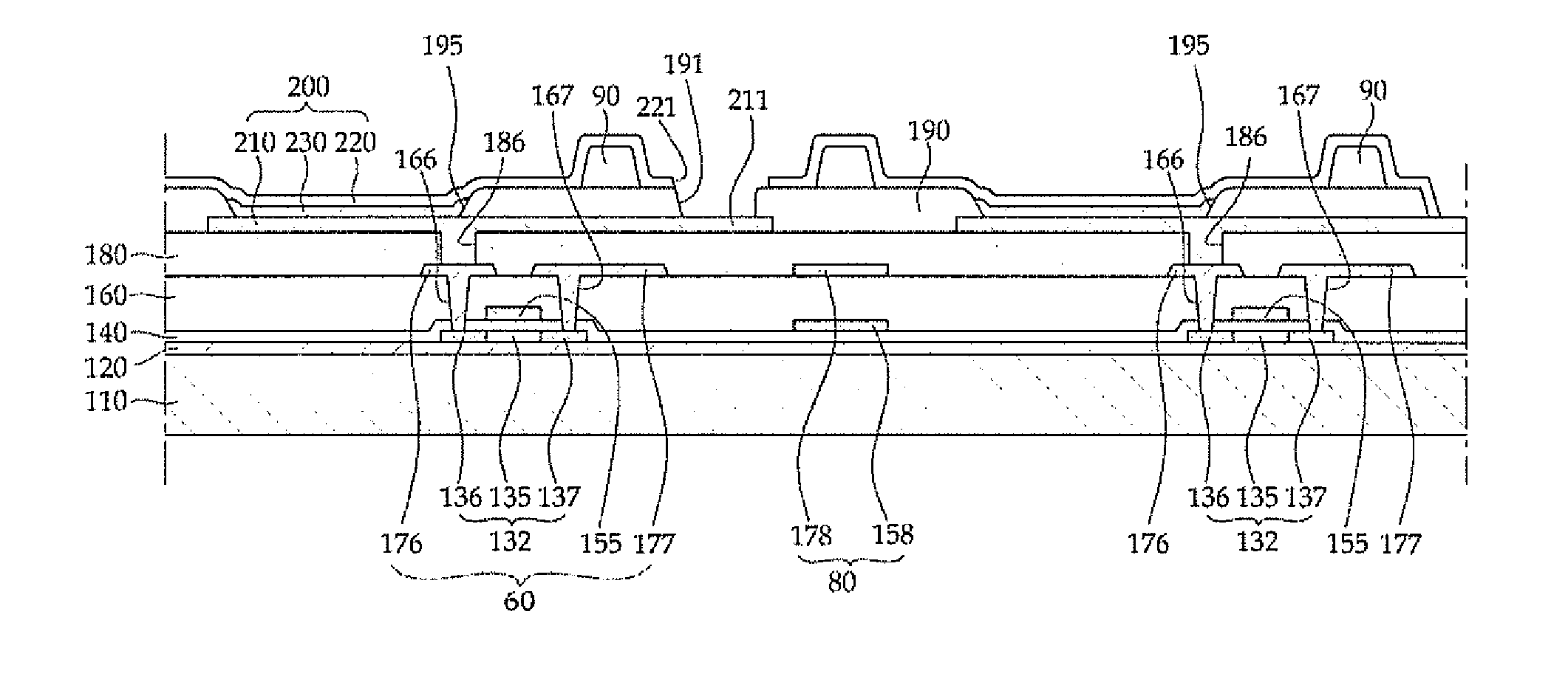
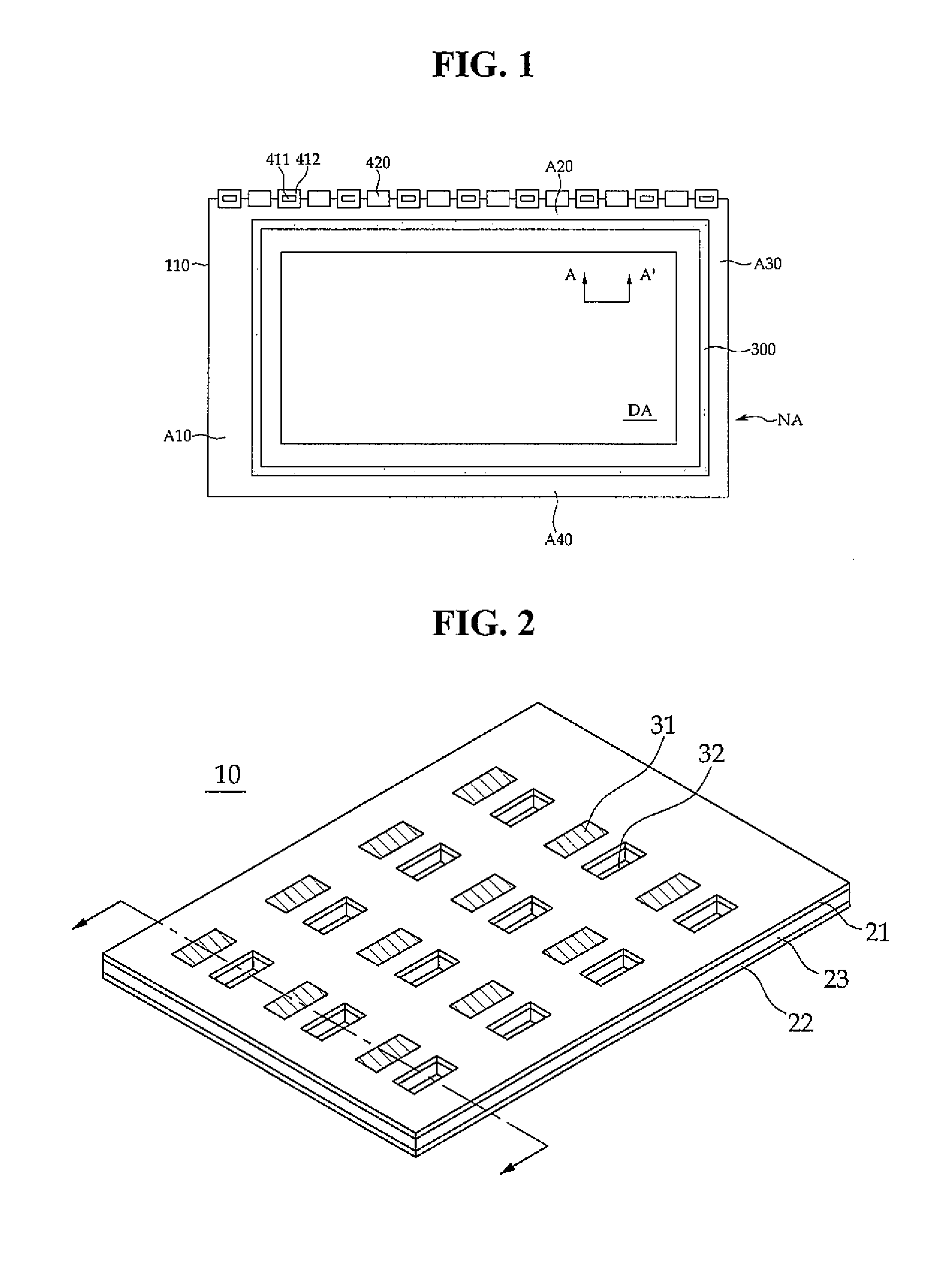
[0048]A display device according to the first embodiment of the present invention will be described below with reference to FIGS. 2 and 3.

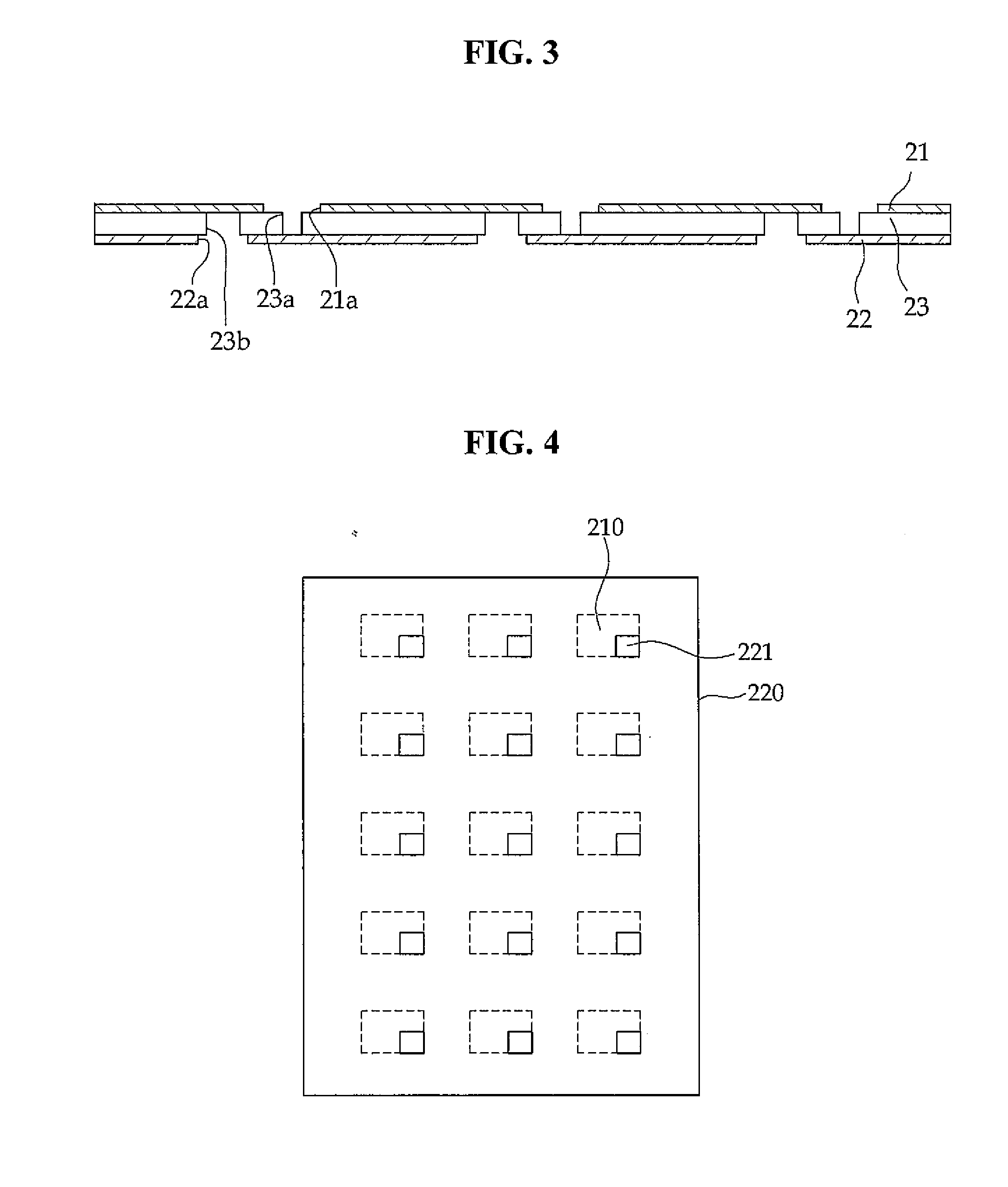
[0049]FIG. 2 is a schematic plan view illustrating a sealing member 10 according to the first embodiment of the present invention. FIG. 3 is a cross-sectional view of the sealing member 10 illustrated in FIG. 2, taken along line B-B′ of FIG. 2.

[0050]Referring to FIGS. 2 and 3, the sealing member 10 includes a first conductive layer 21, a second conductive layer 22, an insulating layer 23, a first conductive layer contact area 31, and a second conductive layer contact area 32.

[0051]The sealing member 10 has a size for covering a display area DA (e.g., all of the display area DA) except for a pad area A10 of a non-display area NA. For example, the sealing member 10 has a size for covering all three line areas A20, A30, and A40. The sealing member 10 covers pixels inside the sealing member 300, and the sealing...

Example

Second Embodiment of the Present Invention

[0094]Hereinafter, a second embodiment of the present invention will be described with reference to FIG. 7. According to the second embodiment of the present invention, first drive power is applied to a first electrode in the same (or substantially the same) manner as the first embodiment of the present invention discussed above, and second drive power is applied to a second electrode through a pad in a non-display area NA outside of a display area DA. Below is a description of elements that are different from those of the first embodiment. Elements that are the same (or substantially the same) as those described above with respect to the first embodiment are not described again here.

[0095]FIG. 7 is a cross-sectional view illustrating portions of a display device according to the second embodiment of the present invention.

[0096]Referring to FIG. 7, a third pad 52 is disposed in a pad area A10 of the non-display area NA. According to the seco...

Example

Third and Fourth Embodiments of the Present Invention

[0099]Hereinafter, third and fourth embodiments of the present invention will be described with reference to FIGS. 8 and 9. Below is a description of configurations of first and second electrodes 210 and 220 that are different from those of the first embodiment of the present invention discussed above. Elements that are the same (or substantially the same) as those described above with respect to the first embodiment are not described again here.

[0100]FIG. 8 is a schematic plan view illustrating first and second electrodes according to the third embodiment of the present invention. FIG. 9 is a schematic plan view illustrating first and second electrodes according to the fourth embodiment of the present invention.

[0101]Referring to FIG. 8, the second electrode 220 may have a larger through hole 221 than that of the first embodiment of the present invention. Therefore, a first conducting member 41 may also be larger, and the first e...


PUM


Abstract

A display device includes a first substrate including a display area and a non-display area, the display area including a pixel including a first electrode, a light emission layer, and a second electrode; a sealing member facing the first substrate; and a first conducting member in the display area, the first conducting member being coupled to the first electrode, where the sealing member includes: a first conductive layer coupled to the first conducting member; an insulating layer on the first conductive layer; and a second conductive layer on the insulating layer, the second conductive layer being coupled to the second electrode.

Description

CROSS-REFERENCE TO RELATED APPLICATION[0001]This application claims priority to and the benefit of Korean Patent Application No. 10-2014-0021396, filed on Feb. 24, 2014, in the Korean Intellectual Property Office, the entire content of which is incorporated herein in its entirety by reference.BACKGROUND[0002]1. Field[0003]Aspects of embodiments of the present invention are directed toward a display device in which driving voltage is applied to first and second electrodes in a display unit using (utilizing) a sealing member.[0004]2. Description of the Related Art[0005]In general, flat panel displays, such as liquid crystal displays and organic light emitting diode displays, include a plurality of pairs of electric field generating electrodes and an electro-optical active layer interposed therebetween. In the case of the liquid crystal display, a liquid crystal layer is included as the electro-optical active layer, and in the case of the organic light emitting diode display, an organi...

Claims


Application Information

Patent Timeline
IPC IPC(8): H01L27/12H01L23/00
CPCH01L23/564H01L27/124H10K59/122H10K59/131H10K50/8423H10K50/8428
Inventor JUNG, HAE-GOORYU, DO-HYUNGSONG, JAE-WOOLEE, JAE-HOON
Owner SAMSUNG DISPLAY CO LTD
Why Eureka
Try Eureka