Prevention of warping during handling of chip-on-wafer

Inactive Publication Date: 2015-09-03
IBM CORP
View PDF4 Cites 0 Cited by
  • Summary
  • Abstract
  • Description
  • Claims
  • Application Information

AI Technical Summary

Benefits of technology

The present invention provides methods for preventing warping of a TSV wafer during handling before and after thinning. The methods involve arranging chips on the TSV wafer, fixing the chips to the wafer, sealing the spaces between the chips, adding a support, melting solder bumps, arranging solder bumps on the bottom surface of the wafer, melting the solder bumps, and dicing the wafer. These methods can help to maintain the shape and quality of the TSV wafer, which can improve the efficiency of the manufacturing process and ultimately improve the performance of the finished products.

Problems solved by technology

Therefore, the wafers easily warp when the wafers are handled before being cut into small pieces by dicing, and there is a risk that warping or breakage will occur unless the wafers are handled very carefully.
It is difficult to form TSVs having a large aspect ratio in a process of forming the TSVs in a TSV wafer or a TSV chip.
On the other hand, it is technically difficult to cut via holes and fill them so as to increase β. This is the reason why it is difficult to increase the aspect ratio of the TSVs.
If TSVs having a large diameter are formed, there is a risk that device performance will be degraded owing to an internal stress caused by a difference in coefficient of linear expansion between the material of the TSVs and the material of the wafer, that is, silicon.
The warping of the TSV chips causes a problem of, in particular, a bonding failure in a chip bonding process performed in a reflow oven. FIG. 2 illustrates the problem that warping of a TSV chip causes a bonding failure in a chip bonding process performed in a reflow oven in manufacturing of a three-dimensional stacked device.
In addition, because the thin TSV chip warps by a large amount owing to a difference in coefficient of thermal expansion (CTE) between the TSV chip and the organic substrate, it is difficult to mount a top chip onto the TSV chip by a reflow process.
This makes the procedure impractical from the viewpoint of process cost.
Neither of the procedures illustrated in FIGS. 2(a) and 2(b) can easily solve the problem that a bonding failure, including a bonding displacement or breakage of a chip, occurs in a reflow bonding process for bonding the chip, and it is difficult to solve this problem.
However, in particular, past technologies do not provide for the “preparation of a silicon wafer in which TSVs do not extend to a bottom surface of the silicon wafer, and scraping of the bottom surface so that the TSVs extend to the bottom surface while a support is fixed to the silicon wafer.”

Method used


Image

  • Prevention of warping during handling of chip-on-wafer
  • Prevention of warping during handling of chip-on-wafer
  • Prevention of warping during handling of chip-on-wafer

Examples


first embodiment

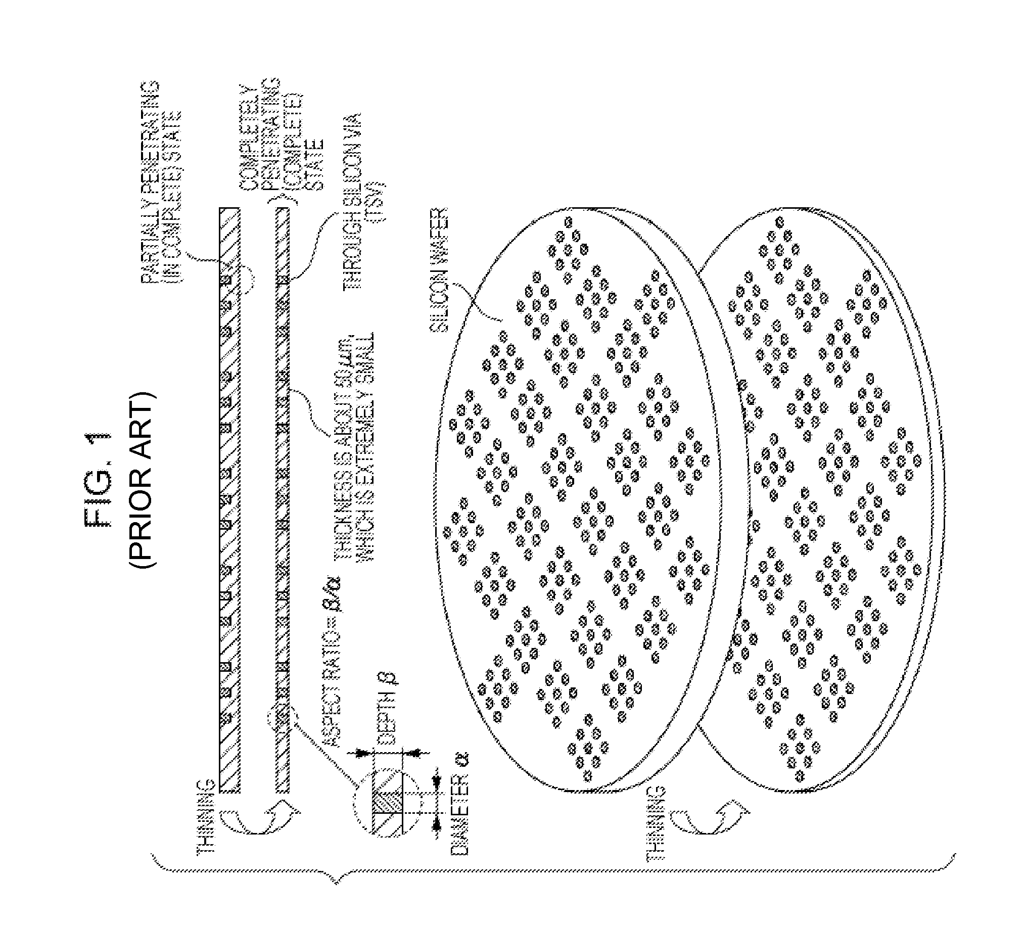
[0023]FIG. 3 illustrates a process according to the present invention. In step A1, a silicon wafer in which TSVs do not extend to one of top and bottom surfaces of the silicon wafer and are in a partially penetrating, or incomplete, state is prepared. The wafer in this state can be referred to as a “TSV wafer (before thinning)” or a “wafer before thinning”.

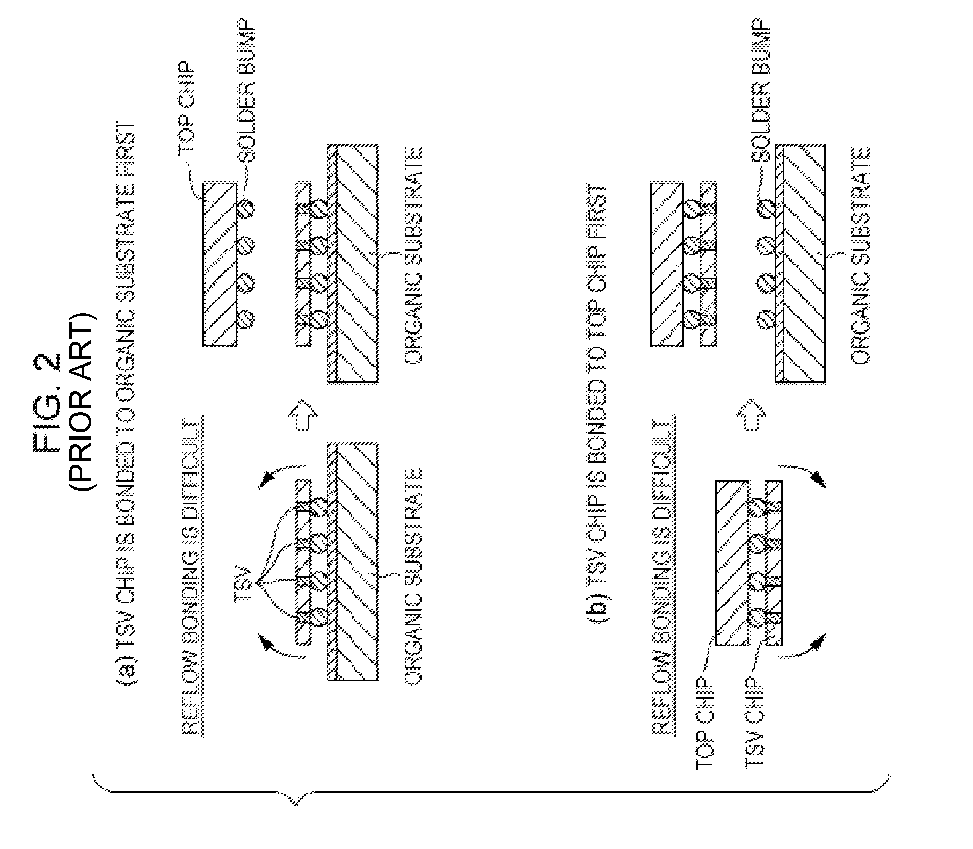
[0024]A plurality of chips, which have already been tested and completed, are arranged so as to correspond to the TSVs, and are fixed by melting a plurality of solder bumps. It is assumed that the chips are simultaneously bonded in a reflow oven after being provisionally fixed with a flux. However, the method for bonding the chips is not limited to this, and the chips may also be stacked in multiple stages. The chips can be those that have already been tested and completed. A space between each chip and the silicon wafer is sealed with an underfill material. Since the space is sealed, sufficient resistance to an external mechanica...

second embodiment

[0031]A resin curable by light, heat, or the like, can be used in the molding process. The support provisionally fixing layer can be formed by, for example, a spin-coating technology. FIG. 5 illustrates a process according to the present invention. In step C1, a silicon wafer in which TSVs extend to both top and bottom surfaces of the silicon wafer and are in a completely penetrating state is prepared. The wafer in this state can be referred to as a “thinned wafer” or a “wafer after thinning.” A plurality of chips, which have already been tested and completed, are arranged on the top surface of the silicon wafer so as to correspond to the TSVs, and are fixed by melting a plurality of solder bumps. The chips can be those that have already been tested and completed. A space between each chip and the silicon wafer is sealed with an underfill material. In step C2, a support is fixed so as to cover the fixed and sealed chips. The support increases the rigidity. In step C3, solder bumps a...

third embodiment

[0035]FIG. 7 illustrates a process according to the present invention. In step E4, a piece of dicing tape is prepared before the wafer is diced, and the solder bumps fixed to the bottom surface of the wafer are placed on the piece of dicing tape. The piece of dicing tape itself can have a reinforcing function. Variations in height caused by variations in diameter of the solder bumps can be absorbed by the piece of dicing tape.

[0036]Although the support is removed in step E4, dicing is preferably performed while the piece of dicing tape is attached in the state where the support is not yet removed—in other words, while the original function of the dicing tape is achieved. In step E5, the piece of dicing tape is removed. It can be effective to apply a release agent or the like in advance. Instead of removing the piece of dicing tape, the main body can be removed from the piece of dicing tape.

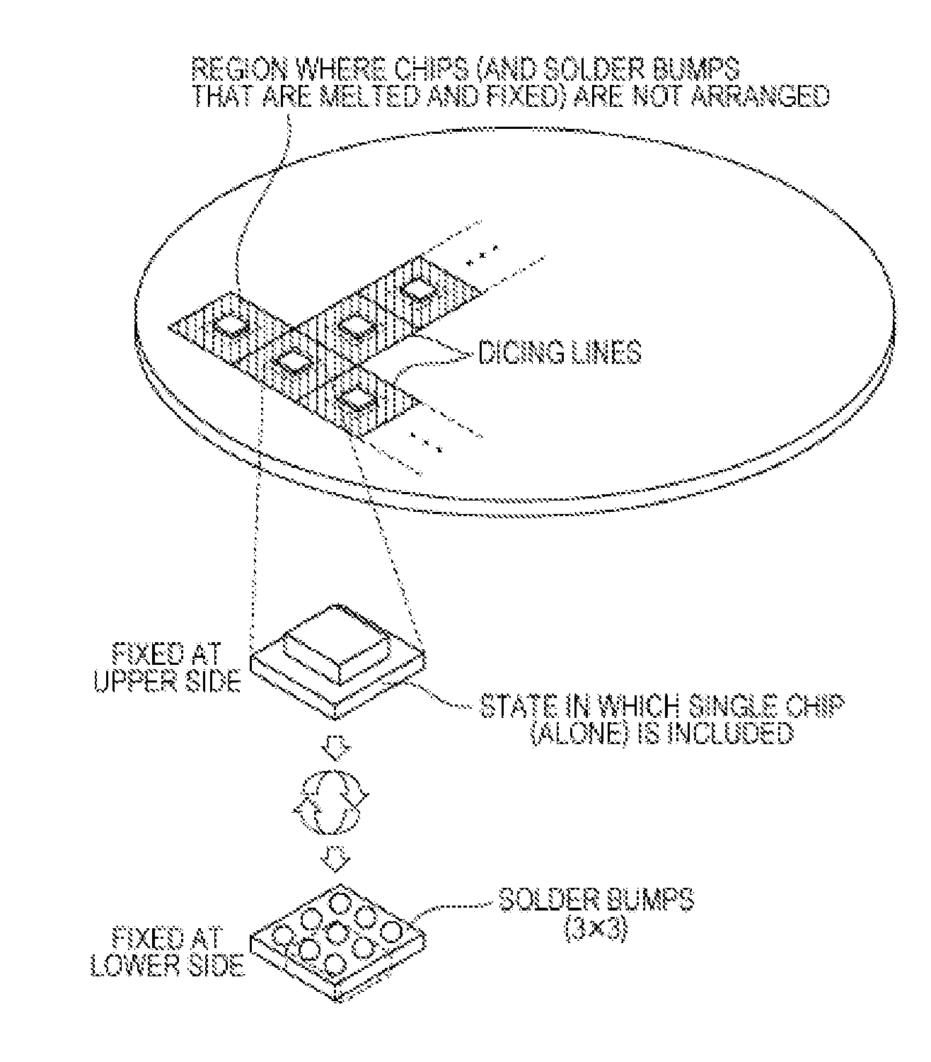
[0037]FIG. 8 illustrates an application process according to the third embodiment of the prese...


PUM


Abstract

To reduce the risk of reduction in yield due to breakage of a thin wafer or a thin chip having through silicon vias (TSVs) formed therein in a chip bonding process, and to prevent warping during handling of a chip-on-wafer (CoW). Chips are bonded to a wafer having TSVs formed therein and sealed before the wafer is thinned. Subsequently, the CoW is subjected to a process of thinning the TSV wafer, a back-surface treatment, and a process of cutting the wafer into small pieces by dicing. Although thin wafers and thin chips having TSVs formed therein are difficult to handle since the chips are bonded to the wafer before thinning and the wafer is thinned and cut into small pieces while mechanical strength thereof is increased by fixing a support to the wafer, the yield of three-dimensional stacked devices can be increased.

Description

BACKGROUND OF THE INVENTION[0001]1. Field of the Invention[0002]The present invention relates to a semiconductor mounting method, and more particularly, to a technology for preventing warping during handling of a chip-on-wafer (CoW).[0003]2. Description of Related Art[0004]A method for producing a three-dimensional mounting device requires a high yield, low cost process. It is desirable to employ an organic substrate and perform solder bonding in a reflow oven to achieve high performance and low cost. A through silicon via (TSV) wafer is a wafer in which TSVs are formed. A TSV chip is a chip in which TSVs are formed.[0005]FIG. 1 illustrates a silicon wafer in which TSVs do not extend to one of top and bottom surfaces of the silicon wafer and are in a partially penetrating, or incomplete state and a silicon wafer in which TSVs extend to both top and bottom surfaces of the silicon wafer and are in a completely penetrating, or complete, state. Silicon wafers are known to be typically d...

Claims


Application Information

Patent Timeline
IPC IPC(8): H01L23/00H01L23/31H01L21/56H01L21/78H01L23/538
CPCH01L24/81H01L21/78H01L24/17H01L2224/81801H01L21/563H01L23/3157H01L23/5384H01L23/3128H01L21/561H01L23/147H01L24/13H01L24/16H01L24/32H01L24/73H01L24/92H01L2224/131H01L2224/32225H01L2224/73204H01L2224/92125H01L2224/97H01L2924/15311H01L2924/157H01L21/486H01L2224/81191H01L2224/8121H01L2224/81815H01L23/49816H01L21/6835H01L23/49827H01L2221/68327H01L2224/16235H01L21/6836H01L24/97H01L2924/3511H01L2224/81H01L2224/83H01L2924/014H01L2924/00014H01L2224/16225H01L2924/00H01L23/3142H01L23/562H01L23/481H01L23/49894H01L24/11H01L2221/68372H01L2224/11334H01L2224/81192H01L2924/01014
Inventor HORIBE, AKIHIROORII, YASUMITSU
Owner IBM CORP
Why Eureka
Try Eureka