Thermoelectric device

a technology of thermoelectric devices and electrons, applied in the direction of thermoelectric devices with peltier/seeback effect, basic electric elements, electric apparatus, etc., can solve the problem of difficulty in realizing a thermoelectric device having high power factor, and achieve the effect of increasing electron density, increasing power factor, and increasing electron density

Active Publication Date: 2015-09-10
TDK CORPARATION
View PDF2 Cites 4 Cited by
  • Summary
  • Abstract
  • Description
  • Claims
  • Application Information

AI Technical Summary

Benefits of technology

[0009]In the stacked structure, the addition of a specified element to the carrier supply layer can increase electric conductivity while suppressing a decrease in Seebeck coefficient, and thus power factor can be improved.
[0010]Further, the stacked thermoelectric thin film preferably has a plurality of stacked structures each having the first high-purity layer and the composite carrier supply layer. This makes it easy to obtain high electric power, for example, in application to thermoelectric power generation.
[0011]Further, at least one of the rocking-curve half widths of a 0th order peak corresponding to the average lattice constant of a superlattice of the stacked thermoelectric thin film and satellite peaks of the 0th-order peak observed by X-ray diffraction measurement is preferably 0.1° or less. The stacked structure having such crystallinity can realize higher power factor.
[0013]Further, each of the first high-purity layer, the second high-purity layer, and the third high-purity layer preferably has a thickness of 1 nm or more and 50 nm or less. This can increase the electron density in each of the layers and can realize even higher power factor.
[0014]Further, the carrier supply layer preferably has a thickness equal to or larger than the thickness of a monoatomic layer and of 10 nm or less. This can increase the electron density in the carrier supply layer and can realize even higher power factor.

Problems solved by technology

However, even when a hetero-structure including two layers having different band gaps, such as Si / SiGe, is realized, it is difficult to actually realize a thermoelectric device having high power factor.

Method used


Image

  • Thermoelectric device
  • Thermoelectric device
  • Thermoelectric device

Examples


example 1

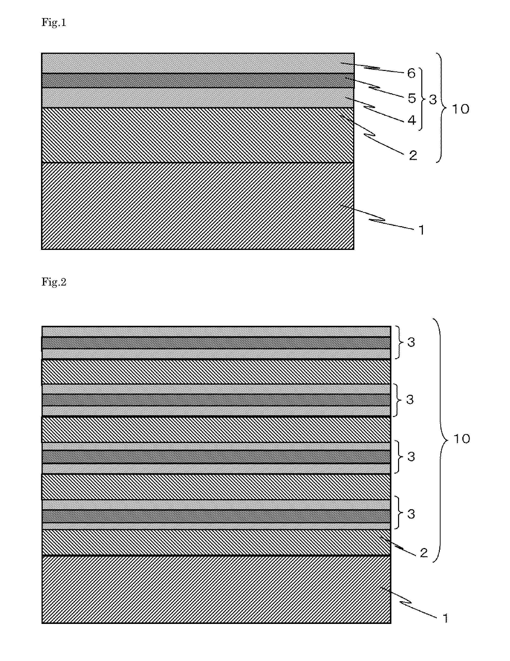
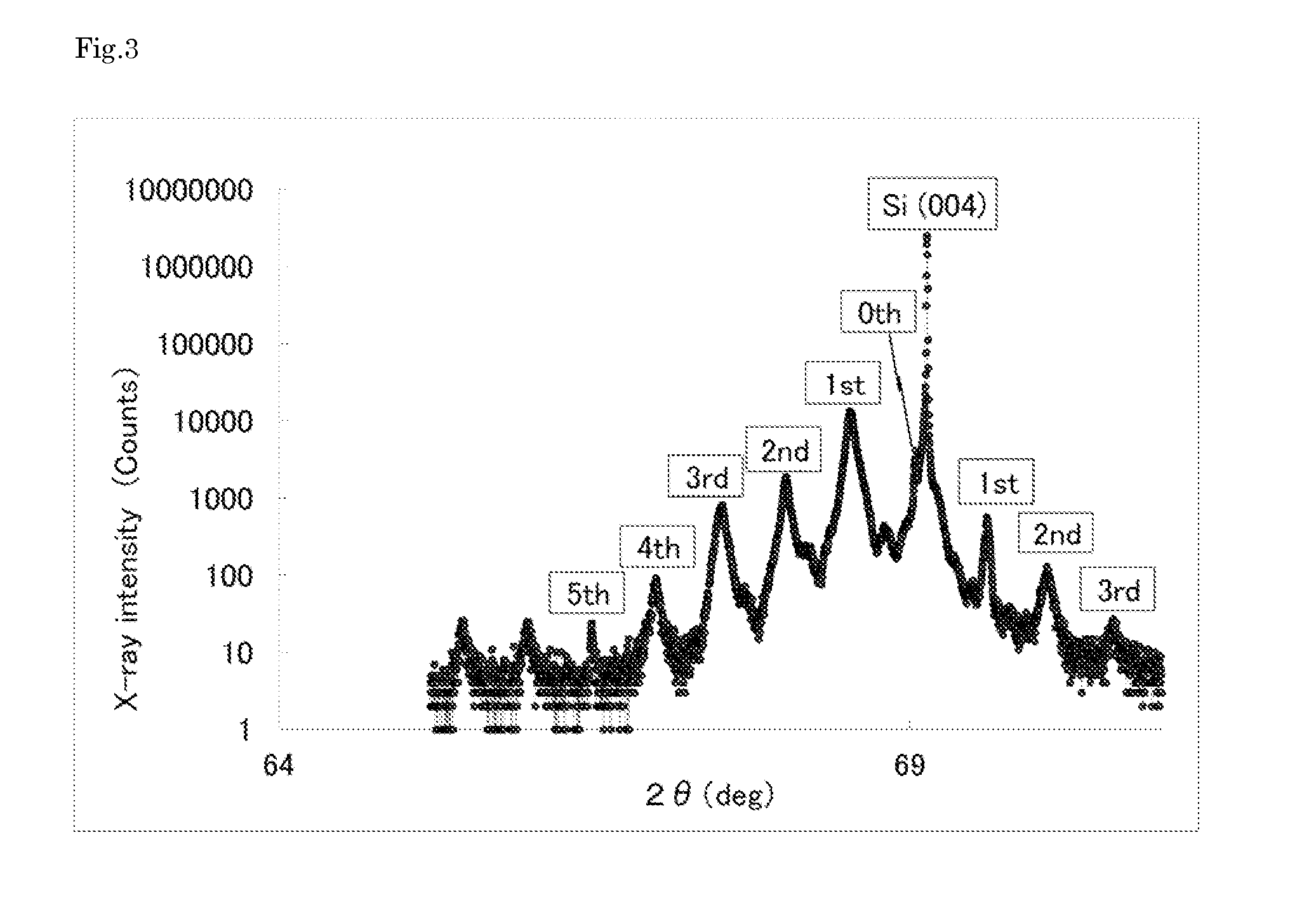
[0058]In Example 1, a sample exclusive for N-type thermoelectric evaluation was formed and evaluated, the sample having characteristics equivalent to those of the thermoelectric device 14 including the stacked thermoelectric thin film 10 according to the second embodiment and the carrier supply layer 5 being doped with Sb. First, the stacked thermoelectric thin film 10 was formed on the substrate 1.

[0059]A Si single crystal substrate was prepared as the substrate 1. The (100) plane of the substrate 1 was used as a deposition surface. The substrate 1 was washed at a high temperature with a concentrated liquid prepared by adding an alkali or acid to a hydrogen peroxide base and then washed with hydrofluoric acid.

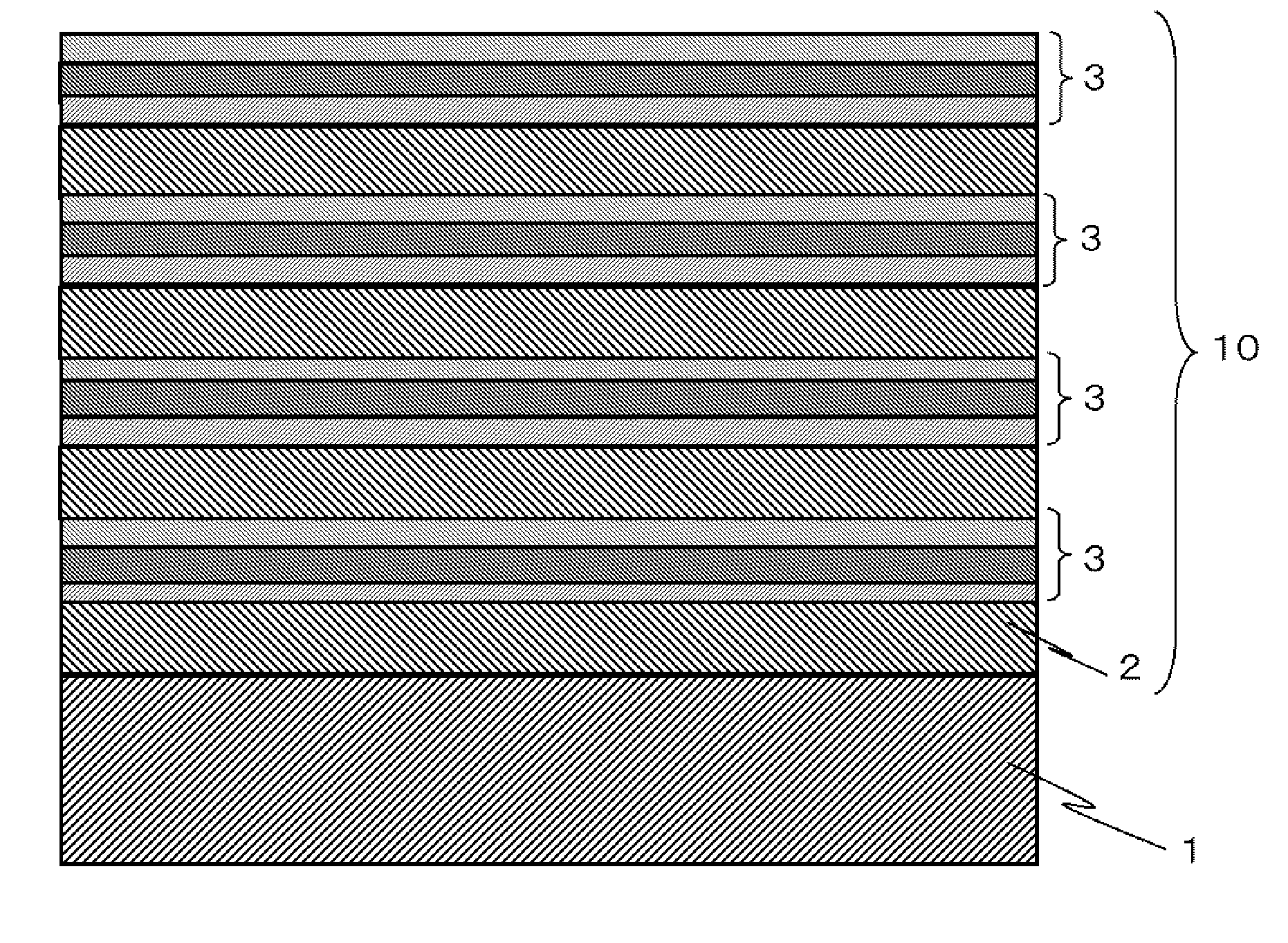
[0060]The stacked thermoelectric thin film 10 was formed on the washed substrate 1. First, SiGe was deposited to form the first high-purity layer 2. The Si:Ge composition ratio was 80:20. The thickness of the SiGe layer was 10 nm.

[0061]Then, the composite carrier supply layer ...

example 2

[0063]In Example 1, the SiGeSb film formed by adding Sb to a SiGe film was deposited as the carrier supply layer 5. However, in Example 2, a SiGeB film was formed by substituting Sb with B, and a sample exclusive for P-type thermoelectric evaluation was formed and evaluated. With the exception of the additive, Example 2 was the same as Example 1.

example 3

[0075]In Example 3, as shown in Table 2, the carrier supply layer 5 including a SiGeSb film formed by adding Sb to a SiGe film had a thickness of 0.5 nm corresponding to the thickness of a monoatomic layer, and the thickness of each of the first high-purity layer 2, the second high-purity layer 4, and the third high-purity layer 6 was changed from 0.8 nm to 55 nm. The value of power factor S2σ in each of the stacked film configurations was confirmed. With the exception of the thicknesses, Example 3 was the same as Example 1. The contents shown in Table 2 reveal that when the thickness of each of the first high-purity layer 2, the second high-purity layer 4, and the third high-purity layer 6 is 1 nm or more and 50 nm or less, a particularly high value of power factor can be achieved.

TABLE 2First high-Second high-CarrierThird high-purity layerpurity layersupply layerpurity layerPowerSiGeSiSiGeSbSifactorthicknessthicknessthicknessthickness(μW / (nm)(nm)(nm)(nm)mK2)Ex-0.80.8Monoatomic0.83...


PUM

PropertyMeasurementUnit
thicknessaaaaaaaaaa
thicknessaaaaaaaaaa
thicknessaaaaaaaaaa

Abstract

A thermoelectric device includes a semiconductor stacked thermoelectric thin film including a first high-purity layer composed of SiGe as a main material and a composite carrier supply layer formed on the first high-purity layer. The composite carrier supply layer includes a second high-purity layer and third high-purity layer composed of Si as a main material, and a carrier supply layer held between the second and third high-purity layers and composed of SiGe as a main material. The carrier supply layer is a P-type carrier supply layer to which an additive of a group XIII element is added or a N-type carrier supply layer to which an additive of a group XV element is added.

Description

BACKGROUND OF THE INVENTION[0001]1. Field of the Invention[0002]The present invention relates to a thermoelectric device having thermoelectric properties.[0003]2. Description of the Related Art[0004]Thermoelectric devices utilizing thermoelectric properties of materials are investigated. Examples of a thermoelectric device using the Seebeck effect include a power-generating device utilizing a temperature difference between the outside air and human bodies, and a power-generating device utilizing waste heat from automotive cars, incinerators, heating devices, or the like. Examples of a thermoelectric devices using the Peltier effect include cooling devices for CPU and a laser medium. In particular, the power generating device utilizing a temperature difference attracts attention as an energy harvesting component.[0005]Thermoelectric devices which have been investigated are bulk-type devices using bulk materials such as bismuth-tellurium (BiTe)-based, lead-tellurium (PbTe)-based, sili...

Claims


Application Information

Patent Timeline
Patent Type & Authority Applications(United States)
IPC IPC(8): H01L35/32
CPCH01L35/325H10N10/855H10N10/857
Inventor MAEKAWA, KAZUYAASATANI, TAKASHI
Owner TDK CORPARATION
Why Eureka
Try Eureka