Semiconductor device and method of manufacturing the same

a semiconductor and semiconductor technology, applied in semiconductor devices, semiconductor/solid-state device details, electrical apparatus, etc., can solve the problems of partial discharge between solder and insulating substrate in the vacant space, inability to reliably secure the assembly region, and inability to form a vacant space. to prevent partial discharge

Active Publication Date: 2015-09-17
MITSUBISHI ELECTRIC CORP
View PDF1 Cites 7 Cited by
  • Summary
  • Abstract
  • Description
  • Claims
  • Application Information

AI Technical Summary

Benefits of technology

[0009]The present invention makes it possible to prevent partial discharge.

Problems solved by technology

Failure of the encapsulation material to flow into the hole and, hence, the formation of a vacant space may therefore result.
There is, therefore, a problem that partial discharge occurs between the solder and the insulating substrate in the vacant space.
There is also a problem that if the diameter of the position recognition hole is increased, it is not possible to reliably secure the region necessary for assembly.

Method used


Image

  • Semiconductor device and method of manufacturing the same
  • Semiconductor device and method of manufacturing the same
  • Semiconductor device and method of manufacturing the same

Examples


embodiment 1

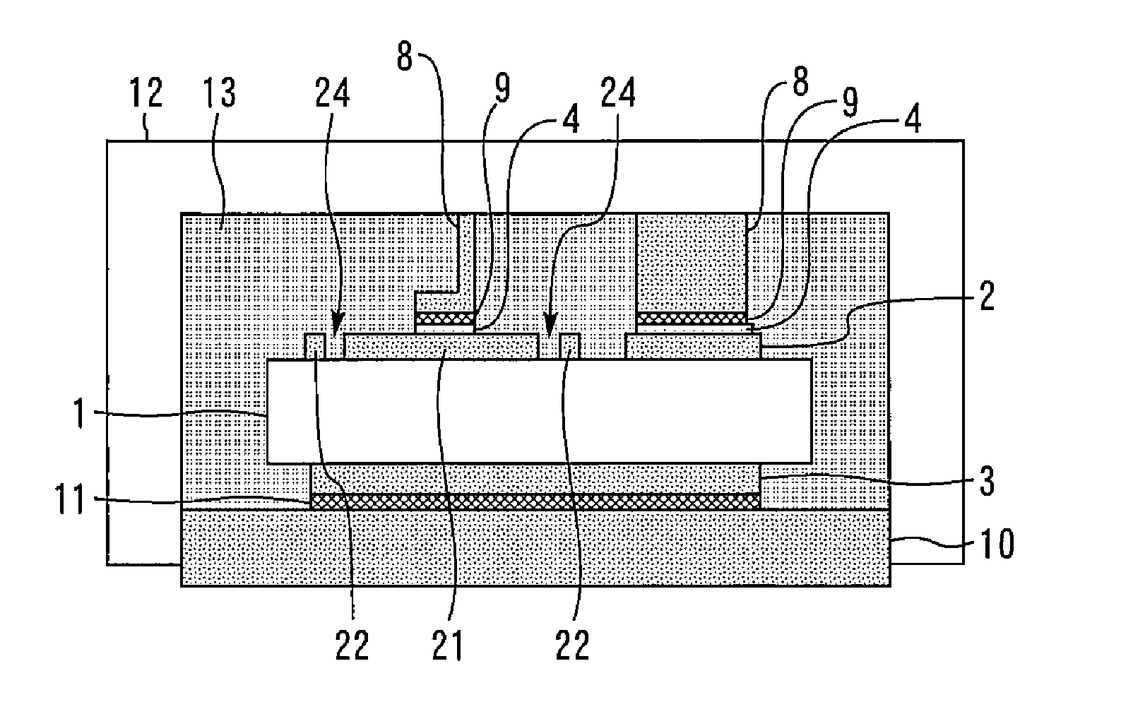
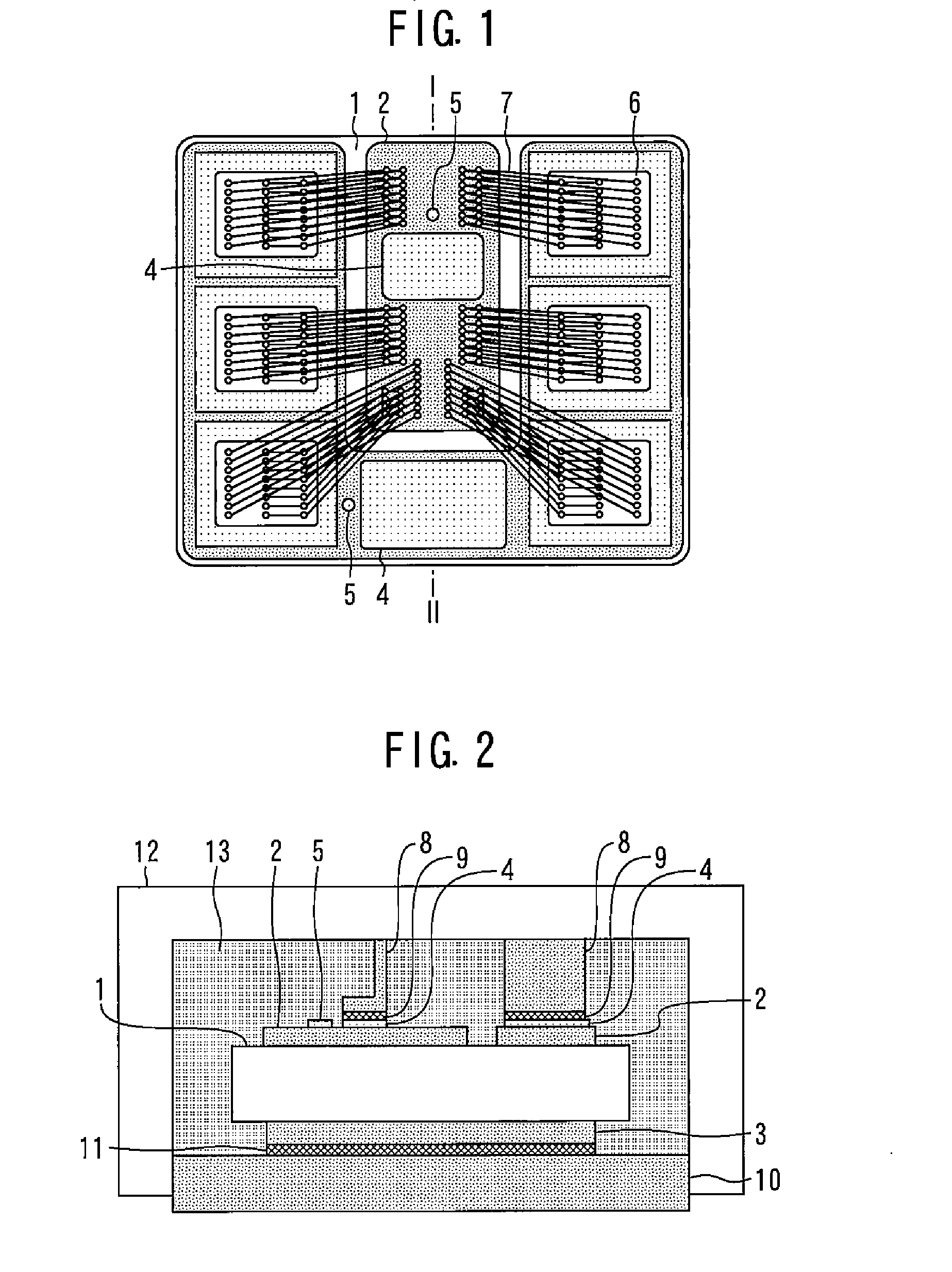
[0077]FIG. 1 is a plan view of a semiconductor device according to Embodiment 1 of the present invention. FIG. 2 is a sectional view taken along line I-II in FIG. 1. Wiring patterns 2 are provided on an upper surface of an insulating substrate 1, while a metal pattern 3 is provided on a lower surface of the insulating substrate 1. Soldering portions 4 are provided on the wiring patterns 2. Ni plating marks 5 are provided in the wiring patterns 2. The soldering portions 4 and the marks are formed of the same material, which is Ni.

[0078]Semiconductor chips 6 are mounted on the insulating substrate 1. Wires 7 are bonded to the semiconductor chips 6. Electrodes 8 are joined to the soldering portions 4 by solder 9. A base plate 10 is joined to the metal pattern 3 by solder 11. All these components are covered with a case 12, and the insulating substrate 1, the semiconductor chips 6, the wires 7 and the electrodes 8 are encapsulated in an encapsulation material 13.

[0079]A method of manufa...

embodiment 2

[0083]FIG. 5 is a plan view of a semiconductor device according to Embodiment 2 of the present invention. FIG. 6 is a sectional view taken along line I-II in FIG. 5. In FIG. 5, illustration of semiconductor chips 6 and wires 7 is omitted.

[0084]A resist mark 15 formed of a solder resist is disposed on a wiring pattern 2 in place of the Ni plating mark 5 in Embodiment 1. A protective film 16 formed of the solder resist covers peripheries of wiring patterns 2. The protective film 16 and the resist mark 15 are simultaneously formed of the solder resist. The position of the insulating substrate 1 is recognized by means of the resist mark 15, and the wires 7 are bonded to the semiconductor chips 6. The other components and process steps are the same as those in Embodiment 1.

[0085]The solder 19 flowing out from the soldering portion 4 does not attach to the resist mark 15 formed of the solder resist, so that no vacant space is formed. Occurrence of partial discharge can thus be prevented. ...

embodiment 3

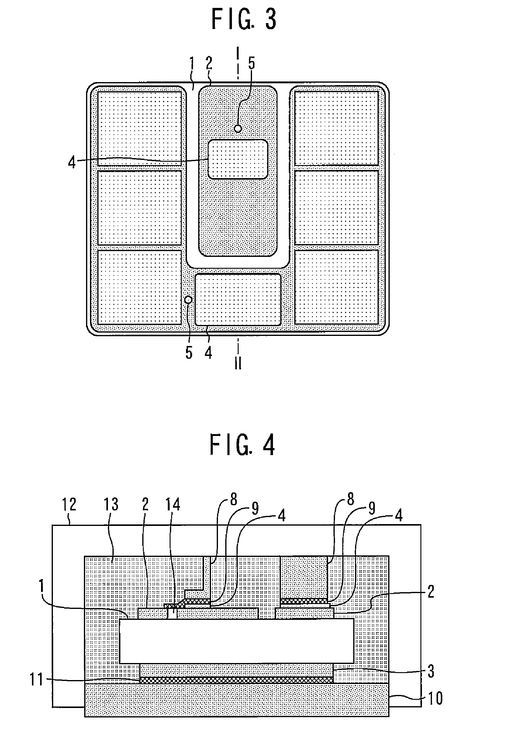
[0086]FIG. 7 is a plan view of a semiconductor device according to Embodiment 3 of the present invention. FIG. 8 is a sectional view taken along line I-II in FIG. 7. In FIG. 7, illustration of semiconductor chips 6 and wires 7 is omitted.

[0087]A protective film 16 formed of a solder resist is provided on the insulating substrate 1. The protective film 16 has openings 17 disposed on the soldering portions 4 and openings 18 disposed on portions other than the soldering portions 4. Electrodes 8 are joined to the soldering portions 4 by solder 9 through the openings 17. The position of the insulating substrate 1 is recognized by means of the openings 18, and the wires 7 are bonded to the semiconductor chips 6. The other components and process steps are the same as those in Embodiment 1.

[0088]The solder 9 flowing out from the soldering portions 4 does not attach to the protective film 16 formed of the solder resist and does not reach either of the openings 18, so that no vacant space is ...


PUM


Abstract

A soldering portion (4) and a Ni plating mark (5) are simultaneously forming by plating on a wiring pattern (2) of an insulating substrate (1). A semiconductor chip (6) is mounted on the insulating substrate (1). A position of the insulating substrate (1) is recognized by the Ni plating mark (5) and a wire (7) is bonded to the semiconductor chip (6). An electrode (8) is joined to the soldering portion (4) by solder (9). The insulating substrate (1), the semiconductor chip (6), the wire (7), and the electrode (8) are encapsulated in an encapsulation material (13).

Description

TECHNICAL FIELD[0001]The present invention relates to a semiconductor device used for electric railway systems, wind power generation, etc., and to method of manufacturing the semiconductor device.BACKGROUND ART[0002]To secure an insulating property of a semiconductor device, an encapsulation material such as silicone gel is injected into the device. Holes for recognition of the position of an insulating substrate in a process step, e.g., wire bonding are provided in a wiring pattern on the insulating substrate (see, for example, Patent Literature 1).CITATION LISTPatent Literature[0003]Patent Literature 1: Japanese Patent Laid-Open No. 2002-299551SUMMARY OF INVENTIONTechnical Problem [0004]If such a position recognition hole exists in the vicinity of a soldering portion, there is a possibility of solder flowing into the hole by flowing out from the soldering portion. When flowing into the hole, the solder is formed into a spherical or disk-like shape by its surface tension. Therefor...

Claims


Application Information

Patent Timeline
Patent Type & Authority Applications(United States)
IPC IPC(8): H01L23/00H01L21/56H01L23/544H01L23/31
CPCH01L24/48H01L23/3107H01L21/56H01L24/85H01L2224/48227H01L2224/8513H01L2224/85801H01L2924/20656H01L2223/54426H01L23/544H01L2224/49111H01L23/60H01L24/49H01L25/072H01L2224/49175H01L2224/92247H01L2224/32225H01L2224/73265H01L23/10H01L23/3128H01L23/3735H01L23/49894H01L2224/83132H01L24/29H01L24/32H01L24/73H01L24/83H01L24/92H01L2223/54486H01L2224/4846H01L2224/49113H01L2224/4917H01L2224/85132H01L2924/00014H01L2224/29101H01L23/5386H01L25/18H01L2924/181H01L2924/00012H01L2224/45099H01L2924/014H01L2924/00H01L2224/85399H01L2224/05599H01L23/12H01L25/07
Inventor MATSUMOTO, TAKAYUKIONISHI, HIROTAKAKOGA, MASUO
Owner MITSUBISHI ELECTRIC CORP
Why Eureka
Try Eureka