Method for manufacturing semiconductor device

Active Publication Date: 2015-09-17
SEMICON ENERGY LAB CO LTD
View PDF8 Cites 48 Cited by
  • Summary
  • Abstract
  • Description
  • Claims
  • Application Information

AI Technical Summary

Benefits of technology

[0007]In a transistor formed using an oxide semiconductor film, oxygen vacancies in a channel region in the oxide semiconductor film cause defects of the electric characteristics of the transistor. For example, the threshold voltage of the transistor that contains oxygen vacancie

Problems solved by technology

In a transistor formed using an oxide semiconductor film, oxygen vacancies in a channel region in the oxide semiconductor film cause defects of the electri

Method used


Image

  • Method for manufacturing semiconductor device
  • Method for manufacturing semiconductor device
  • Method for manufacturing semiconductor device

Examples


embodiment 1

[0073]In this embodiment, embodiments of a semiconductor device and a method for manufacturing the semiconductor device will be described with reference to FIGS. 1A to 1D, FIG. 2, FIGS. 3A to 3D, and FIGS. 4A to 4C.

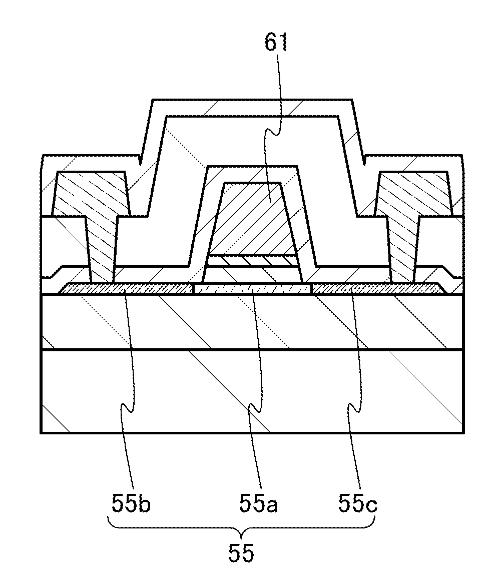
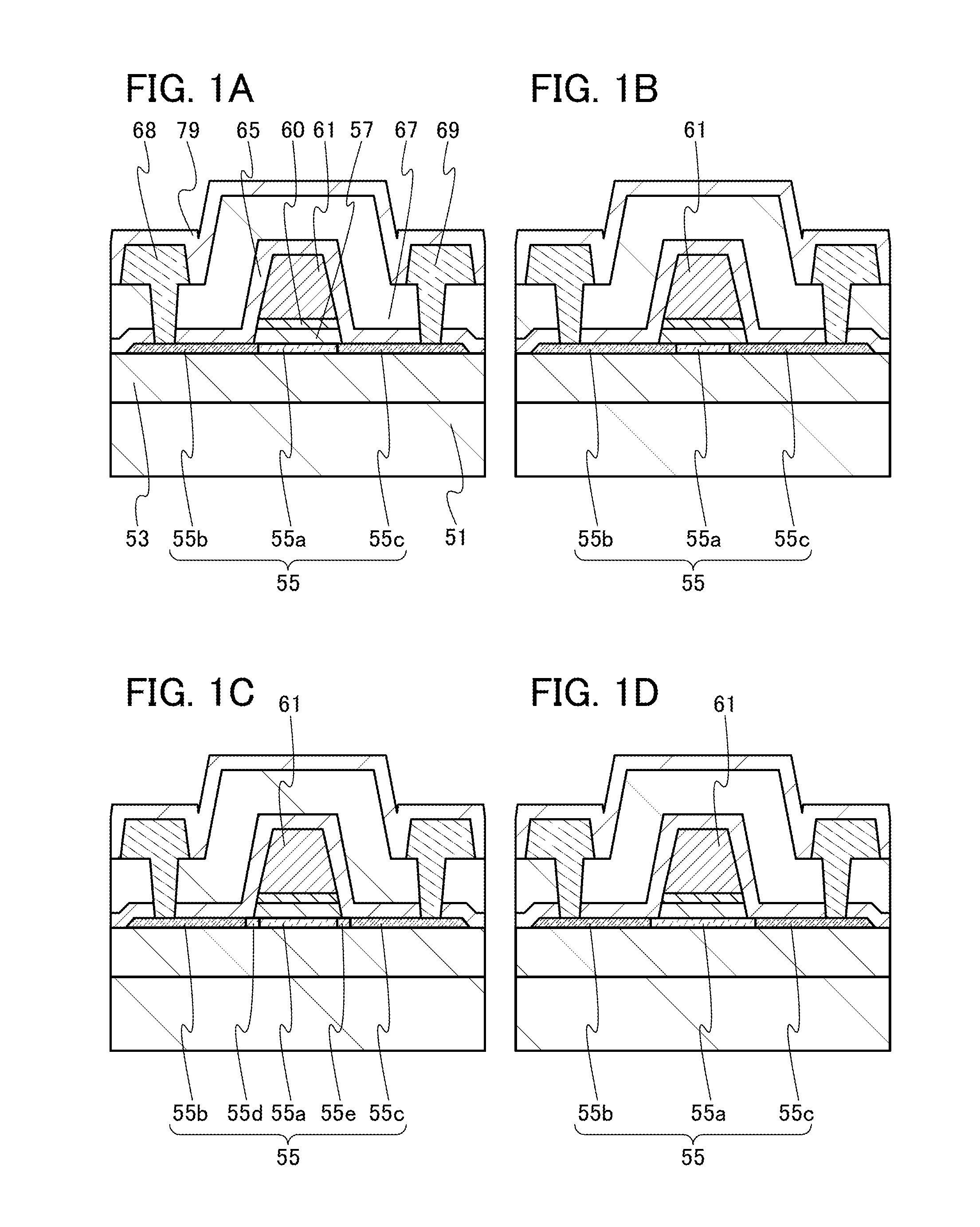
[0074]FIGS. 1A to 1D are each a cross-sectional view of a top-gate self-aligned transistor that is an example of a transistor in a semiconductor device.

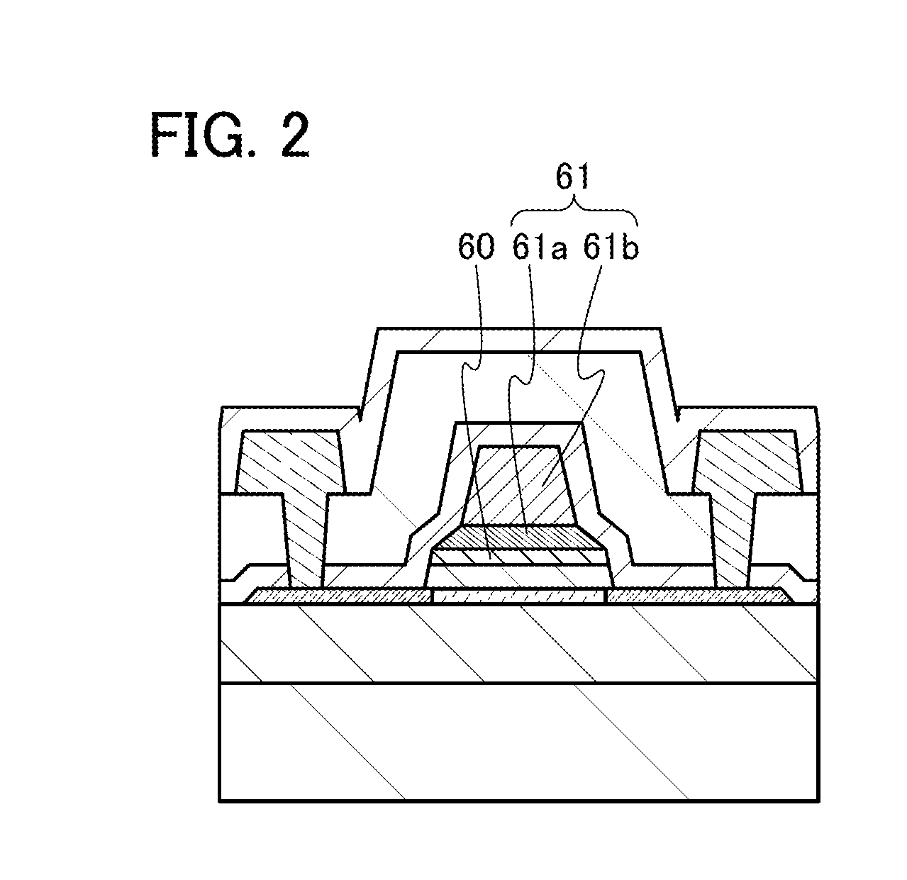
[0075]A transistor illustrated in FIG. 1A includes an oxide semiconductor film 55, an insulating film 57 in contact with the oxide semiconductor film 55, a buffer film 60 over the insulating film 57, and a conductive film 61 in contact with the buffer film 60 and overlapping with the oxide semiconductor film 55.

[0076]The oxide semiconductor film 55 includes a first region 55a and second regions 55b and 55c between which the first region 55a is positioned. The first region 55a has a function of a channel region. The second regions 55b and 55c have functions of a source region and a drain region. Since the resistivity of the...

embodiment 2

[0196]In this embodiment, structures and manufacturing methods of semiconductor devices that are different from those described in Embodiment 1 will be described with reference to FIGS. 5A to 5D, FIGS. 6A to 6D, FIGS. 7A to 7D, FIGS. 8A to 8D, and FIGS. 9A to 9C.

[0197]Transistors described in this embodiment are different from those in Embodiment 1 in that an edge of the buffer film 60 extends beyond the conductive film 61.

[0198]Structures of transistors included in semiconductor devices will be described with reference to FIGS. 5A to 5D.

[0199]A transistor illustrated in FIG. 5A includes the oxide semiconductor film 55, the insulating film 57 in contact with the oxide semiconductor film 55, the buffer film 60 over the insulating film 57, and the conductive film 61 in contact with the buffer film 60 and overlaps with the oxide semiconductor film 55. The edge of the buffer film 60 extends beyond the conductive film 61. This means that the area of the top surface of the buffer film 60 ...

embodiment 3

[0246]In this embodiment, structures and manufacturing methods of semiconductor devices that are different from those described in Embodiments 1 and 2 will be described with reference to FIGS. 3A to 3D, FIGS. 7A to 7D, FIGS. 10A to 10D, FIGS. 11A to 11D, FIGS. 12A to 12D, and FIGS. 13A to 13C.

[0247]Transistors described in this embodiment are different from those described in Embodiments 1 and 2 in that an insulating film containing hydrogen is not formed over the oxide semiconductor film 55 or the insulating film 57.

[0248]Structures of transistors included in semiconductor devices will be described with reference to FIGS. 10A to 10D.

[0249]A transistor illustrated in FIG. 10A includes the oxide semiconductor film 55, the insulating film 57 in contact with the oxide semiconductor film 55, the buffer film 60 over the insulating film 57, and the conductive film 61 in contact with the buffer film 60 and overlaps with the oxide semiconductor film 55.

[0250]The oxide semiconductor film 55 ...


PUM


Abstract

Provided is a method for manufacturing a semiconductor device whose electric characteristics are prevented from being varied and whose reliability is improved. In the method, an insulating film is formed over an oxide semiconductor film, a buffer film is formed over the insulating film, oxygen is added to the buffer film and the insulating film, a conductive film is formed over the buffer film to which oxygen is added, and an impurity element is added to the oxide semiconductor film using the conductive film as a mask. An insulating film containing hydrogen and overlapping with the oxide semiconductor film may be formed after the impurity element is added to the oxide semiconductor film.

Description

BACKGROUND OF THE INVENTION[0001]1. Field of the Invention[0002]The present invention relates to an object, a method, or a manufacturing method. In addition, the present invention relates to a process, a machine, manufacture, or a composition of matter. In particular, one embodiment of the present invention relates to a semiconductor device, a display device, a light-emitting device, a power storage device, a memory device, a driving method thereof, or a manufacturing method thereof. Specifically, one embodiment of the present invention relates to a semiconductor device including a field-effect transistor.[0003]In this specification and the like, a semiconductor device generally means a device that can function by utilizing semiconductor characteristics. A semiconductor element such as a transistor, a semiconductor circuit, an arithmetic device, and a memory device are each an embodiment of a semiconductor device. An imaging device, a display device, a liquid crystal display device,...

Claims


Application Information

Patent Timeline
IPC IPC(8): H01L29/66H01L21/385H01L21/441H01L21/02H01L29/24H01L29/49H01L21/4757H01L29/786H01L21/477
CPCH01L29/66969H01L29/7869H01L21/385H01L21/441H01L21/0217H01L29/24H01L29/4908H01L29/4966H01L21/47573H01L21/477H01L21/02472H01L21/02483H01L21/02554H01L21/02565H01L21/02573H01L21/0262H01L21/02326H01L21/0234H01L29/42384H01L29/78621
Inventor YAMAZAKI, SHUNPEIJINTYOU, MASAMISHIMA, YUKINORI
Owner SEMICON ENERGY LAB CO LTD
Why Eureka
Try Eureka