Electronic component, method of manufacturing the same, and mount structure of electronic component

Active Publication Date: 2015-10-08
MURATA MFG CO LTD
View PDF8 Cites 27 Cited by
  • Summary
  • Abstract
  • Description
  • Claims
  • Application Information

AI Technical Summary

Benefits of technology

[0007]Preferred embodiments of the present invention provide an electronic component with excellent mountability with the use of solder while the oc

Problems solved by technology

As described in International Publication WO2002/082480, ion migration in an electronic component has recently given rise to a problem in some cases.
This problem occurs more noticea

Method used


Image

  • Electronic component, method of manufacturing the same, and mount structure of electronic component
  • Electronic component, method of manufacturing the same, and mount structure of electronic component
  • Electronic component, method of manufacturing the same, and mount structure of electronic component

Examples


first preferred embodiment

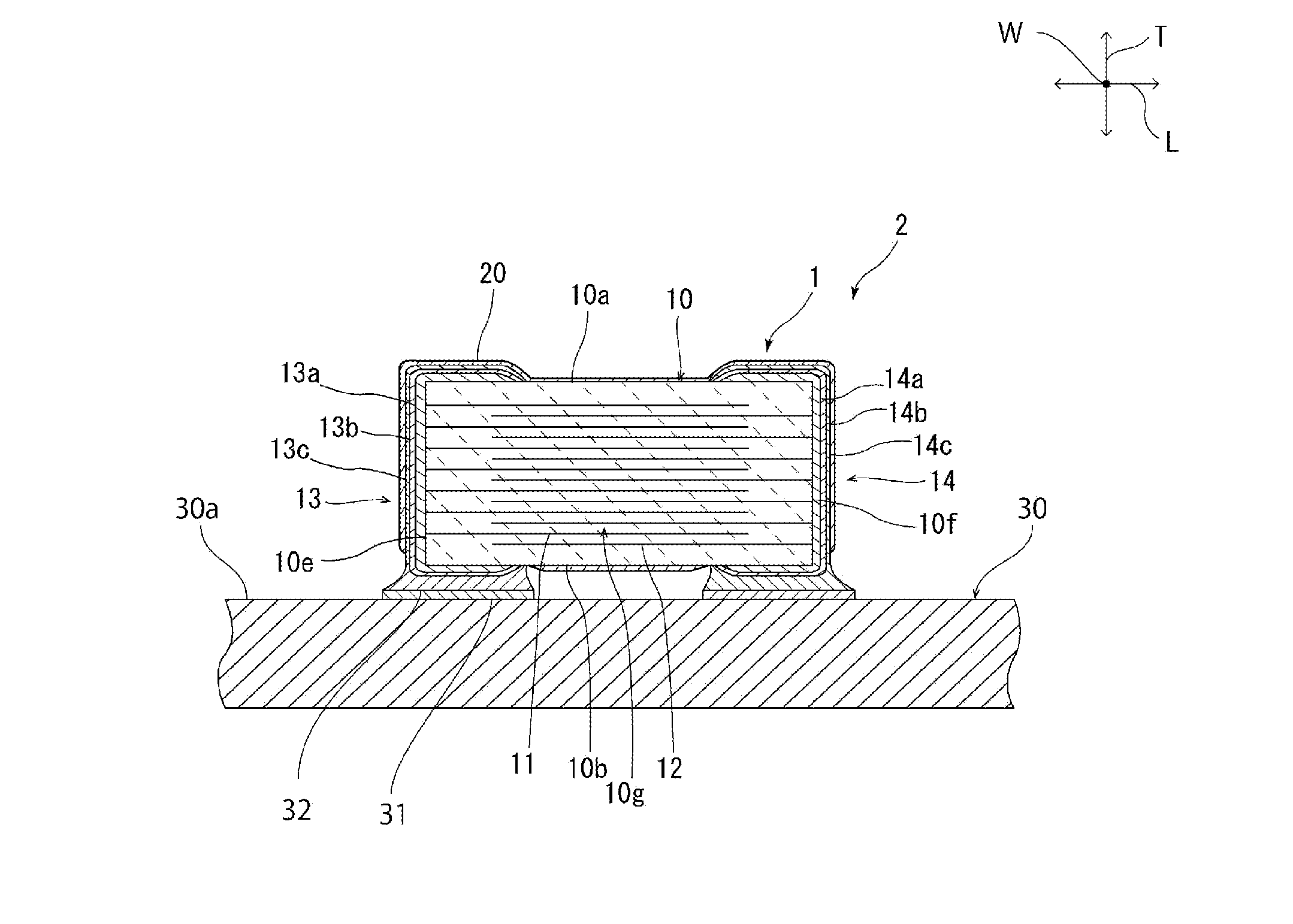
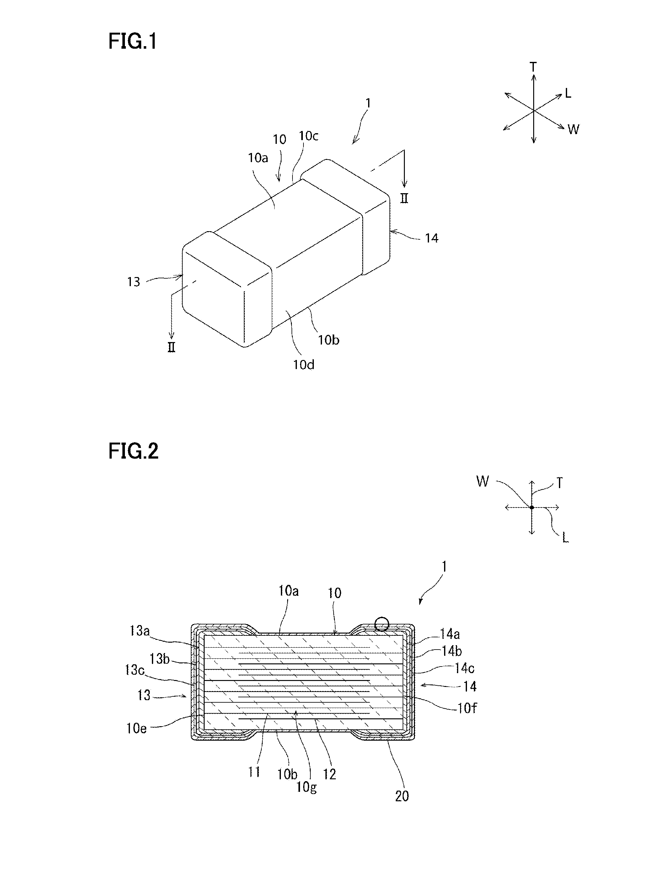
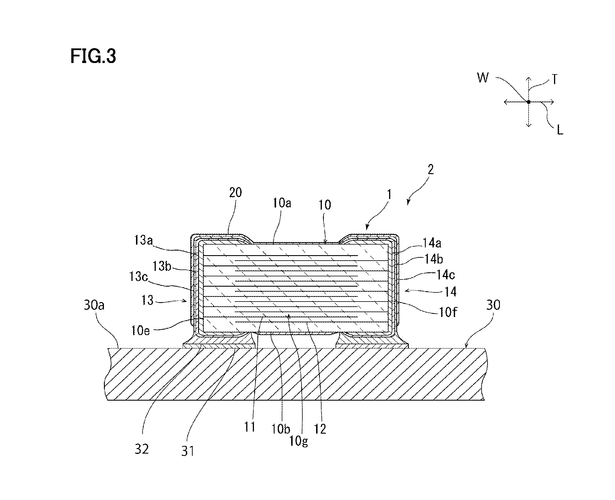
[0034]FIG. 1 is a perspective view showing an electronic component according to a first preferred embodiment of the present invention. FIG. 2 is a cross-sectional view of the electronic component in FIG. 1 viewed in a direction of an arrow II-II. FIG. 1 does not depict a water-repellent film 20.

[0035]As shown in FIGS. 1 and 2, an electronic component 1 includes an electronic component main body 10 preferably having a parallelepiped or substantially parallelepiped shape. An electronic component main body 10 includes first and second main surfaces 10a and 10b, first and second side surfaces 10c and 10d, and first and second end surfaces 10e and 10f. Each of the first and second main surfaces 10a and 10b extends along a length direction L and a width direction W. Each of the first and second side surfaces 10c and 10d extends along a thickness direction T and a length direction L. Each of the first and second end surfaces 10e and 10f extends along a thickness direction T and a width dir...

experimental example 1

[0080]In Experimental Example 1, nine types of electronic components and mount structures of the electronic components in Example 1 to Example 5 and Comparative Example 1 to Comparative Example 4 were fabricated. A stack ceramic capacitor was fabricated as the electronic component.

example 1

[0081]An electronic component and a mount structure of the electronic component according to Example 1 substantially the same as the electronic component 1 according to the first preferred embodiment were fabricated under the conditions described below. A dimension (a design value) of the electronic component was set to about 1.6 mm in length, about 0.8 mm in width, and about 0.8 mm in thickness. A ceramic portion was composed of BaTiO3. The first and second internal electrodes 11 and 12 were composed of Ni. The first electrode layers 13a and 14a were formed from a fired electrode layer containing Cu. The second electrode layers 13b and 14b were formed from a Ni plated layer. The third electrode layers 13c and 14c were formed from a Sn plated layer. A distance along the length direction between the first external electrode 13 and the second external electrode 14 in each of the first and second main surfaces 10a and 10b was set to about 0.8 mm. A liquid obtained by diluting a silicon...


PUM

PropertyMeasurementUnit
Temperatureaaaaaaaaaa
Angleaaaaaaaaaa
Angleaaaaaaaaaa

Abstract

An electronic component includes a main body, first and second external electrodes, and a water-repellent film. The first and second external electrodes are provided on a portion of a surface of the main body. The water-repellent film is provided on another portion of the surface of the main body and on a surface of the first external electrode. The water-repellent film contains a non-cross-linked silicone resin. An angle of contact of water of about 25° C. with the water-repellent film is not less than about 100° and not greater than about 160°.

Description

BACKGROUND OF THE INVENTION[0001]1. Field of the Invention[0002]The present invention relates to an electronic component, a method of manufacturing the same, and a mount structure of an electronic component.[0003]2. Description of the Related Art[0004]Reduction in size and thickness has recently been accelerated in electronic devices such as a portable telephone and a portable music player. Concurrently, for example, reduction in size of an electronic component contained in an electronic device has also been demanded. Such electronic devices are used in various environments, and improvements in the reliability of electronic components in various environments have been desired.[0005]As described in International Publication WO2002 / 082480, ion migration in an electronic component has recently given rise to a problem in some cases. Ion migration occurs, for example, as follows. A temperature difference between an electronic component and outside air causes condensation at a surface of ...

Claims


Application Information

Patent Timeline
IPC IPC(8): H01G4/224H01G4/008H01G4/248H01G4/12H05K1/18H01G4/30
CPCH01G4/224H05K1/181H01G4/30H05K2201/10015H01G4/1245H01G4/008H01G4/248H01G2/065H01G4/232H05K3/3436H05K2201/0769H05K2201/10636Y02P70/50H01G4/2325H01G13/003
Inventor ABE, HIROSHINOMURA, YOSHIYUKISAITO, JUNICHI
Owner MURATA MFG CO LTD
Why Eureka
Try Eureka