Synthetic diamond materials for quantum and optical applications and methods of making the same

a diamond material and quantum optical technology, applied in the field of synthetic diamond materials, can solve the problems of reducing the effective collection efficiency, reducing the absorption cross-section, and affecting the approach of solid-state emitters

Active Publication Date: 2015-10-22
PRESIDENT & FELLOWS OF HARVARD COLLEGE
View PDF2 Cites 62 Cited by
  • Summary
  • Abstract
  • Description
  • Claims
  • Application Information

AI Technical Summary

Benefits of technology

[0038]According to a first aspect of the present invention there is provided a synthetic diamond material comprising one or

Problems solved by technology

When the line width is broader than this transform-limited line width, additional de-phasing leads to a decrease in the absorption cross-section and a decrease in the effective collection efficiency.
The aforementioned approach is problematic for solid state emitters.
One solution to the aforementioned problem is to reduce the resolution of a detector arrangement used to detect photons from photon emitters to an extent that the photons from different sources are indistinguishable to the detectors.
However, the higher timing resolution requires that the count rates in each bin be higher than noise, such as dark counts, and single photon emission from defects in solid state materials can be very weak.
Due to poor collection efficiency only approximately 0.1-1% of this emission is typically detected resulting in low count rates.
Such count rates are insufficient for the realization of advanced quantum information processing protocols within reasonable data acquisition times based on photon interference using high time resolution.
In fact, the aforementioned issues are so problematic that multi-photon quantum interference from multiple solid state quantum registers had not been demonstrated in practice until 2011 (Phys. Rev. Lett. 108, 043604 (2012).
However, multi-photon quantum interference from multiple spin resolved solid state quantum registers has not been demonstrated in practice to date due to the previo

Method used


Image

  • Synthetic diamond materials for quantum and optical applications and methods of making the same
  • Synthetic diamond materials for quantum and optical applications and methods of making the same
  • Synthetic diamond materials for quantum and optical applications and methods of making the same

Examples


Embodiment Construction

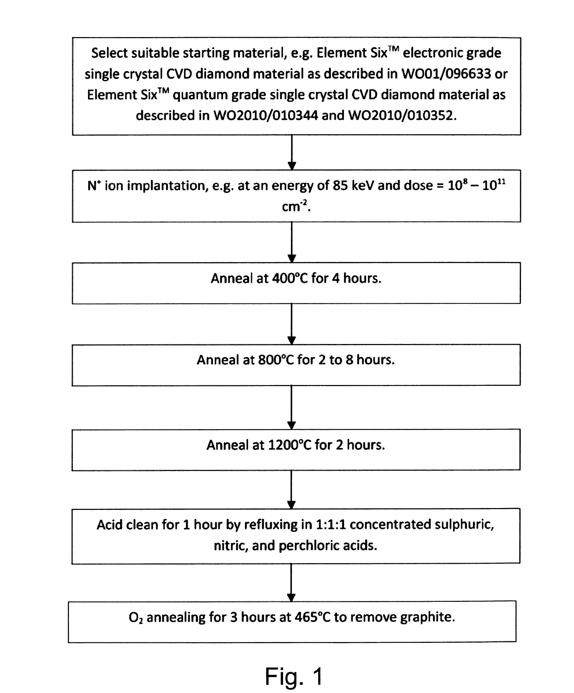
[0055]Embodiments of the present invention provide a route for synthesising solid state emitters with a zero phonon line width approaching that of the transform limited value and which is stable over time with minimal spectral diffusion. As indicated in the summary of invention section, a synthetic diamond material has been fabricated comprising spin defects having a full width half maximum intrinsic inhomogeneous zero phonon line width of less than 100 MHz. This has been achieved by a combination of: (i) selection of a suitable synthetic diamond material; and (ii) treatment of the selected synthetic diamond material using a multistage annealing technique.

[0056]The synthetic diamond material utilized as the staring material for fabricating the aforementioned is preferably a CVD synthetic diamond material and particularly a high purity, low strain CVD synthetic diamond material such as is described in WO01 / 096633, WO2010 / 010344, and WO2010 / 010352. These materials have a single substi...


PUM

PropertyMeasurementUnit
Temperatureaaaaaaaaaa

Abstract

A synthetic diamond material comprising one or more spin defects having a full width half maximum intrinsic inhomogeneous zero phonon line width of no more than 100 MHz. The method for obtain such a material involves a multi-stage annealing process.

Description

FIELD OF INVENTION[0001]The present invention relates to synthetic diamond materials for quantum and optical applications (e.g. quantum optics, quantum information processing, quantum key distribution, single photon sources, quantum repeaters, and / or quantum based sensing devices such as magnetometers) and methods of making the same. Certain embodiments relate to methods of synthesising and subsequently treating diamond materials in order to provide improved emission characteristics from spin defects disposed within the synthetic diamond materials. Particular embodiments relate to chemical vapour deposited (CVD) diamond materials.BACKGROUND OF INVENTION[0002]Quantum emitters (including alkali atoms, trapped ions, solid state defects, and quantum dots) strongly coupled to photons have a wide range of technological applications in photonic computing, quantum information processing, quantum sensing and metrology, and quantum networks. The requirements for most of these applications are...

Claims


Application Information

Patent Timeline
IPC IPC(8): C30B1/04G06N99/00G01N21/64C30B29/04C30B30/00
CPCC30B1/04C30B29/04C30B30/00G01N2021/6497G06N99/002B82Y10/00G01N21/64C30B33/02C30B25/02G06N10/00C01B32/28G02B6/1225H01L31/028H01L33/0054
Inventor MARKHAM, MATTHEWSTACEY, ALASTAIRDELEON, NATHALIECHU, YIWENSHIELDS, BRENDAN JOHNHAUSMANN, BIRGIT JUDITH MARIAMALETINSKY, PATRICKEVANS, RUFFIN ELEYYACOBY, AMIRPARK, HONGKUNLONCAR, MARKOLUKIN, MIKHAIL D.
Owner PRESIDENT & FELLOWS OF HARVARD COLLEGE
Why Eureka
Try Eureka