Omnidirectional high chroma red structural color with semiconductor absorber layer

Active Publication Date: 2015-10-29
TOYOTA JIDOSHA KK
View PDF2 Cites 7 Cited by
  • Summary
  • Abstract
  • Description
  • Claims
  • Application Information

AI Technical Summary

Benefits of technology

[0009]The semiconductor absorber layer can have a thickness between 5-500 nm, inclusive, and be made from such materials such as amorphous silicon (Si), germanium (Ge), and combinations thereof. The thickness of the high index of refraction dielectric layer is greater than 0.1 quarter wave thickness (QW) and less than or equal to 4 QW for a target wavelength, the target wavelength having a predefined hue within the 0-40° on the a*b* Lab color map. The high index of refraction dielectric layer can be made from a dielectric material such as zinc sulfide (ZnS), titanium dioxide (TiO2), hafnium oxide (HfO2), niobium oxide (Nb2O5), tantalum oxide (Ta2O5), and combinations thereof.
[0010]The reflective core layer and semiconductor absorber layer can be dry deposited layers, whereas the high index of refraction dielectric layer can be a wet deposited layer. In addition, the reflective core layer can be a central reflective core layer and the semiconductor absorber layer be a pair of semiconductor absorber layers tha

Problems solved by technology

As such, the cost associated with the production of high-chroma omnidirectional structural colors using multilayer stacks of dielectric materials can be prohibitive.
In particular, the control of angular ind

Method used


Image

  • Omnidirectional high chroma red structural color with semiconductor absorber layer
  • Omnidirectional high chroma red structural color with semiconductor absorber layer
  • Omnidirectional high chroma red structural color with semiconductor absorber layer

Examples


Example

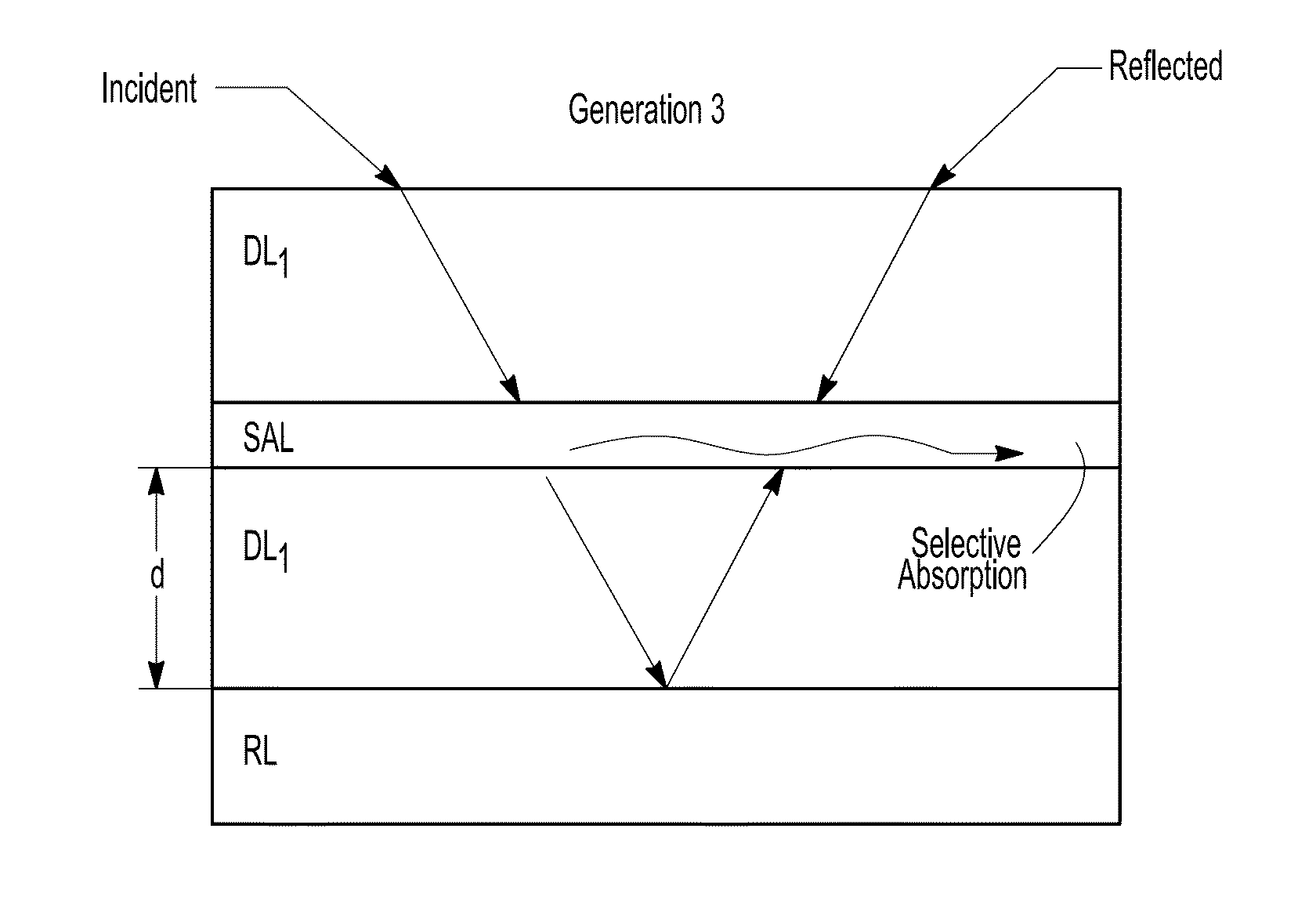
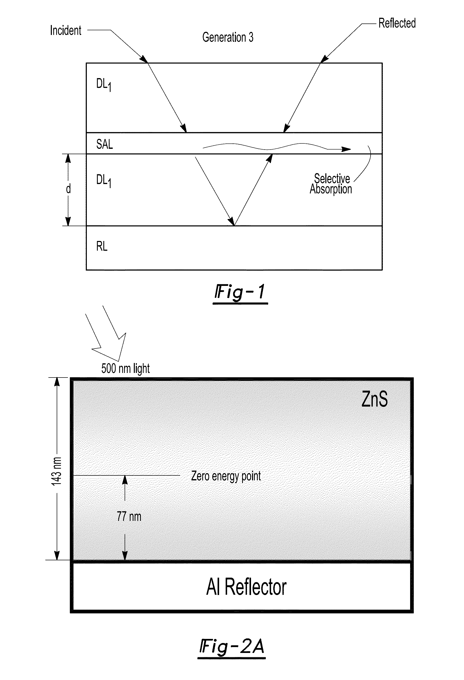
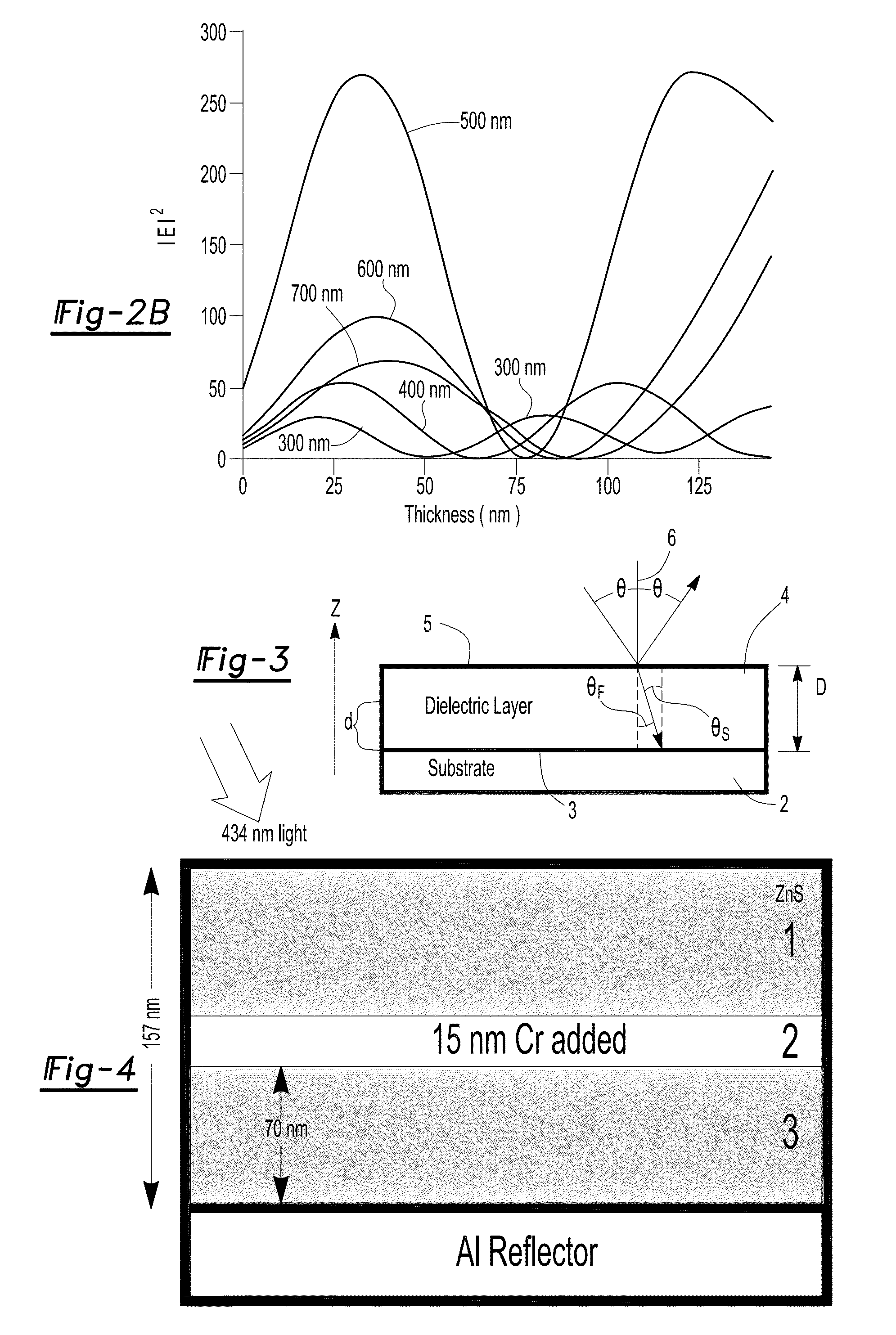
[0038]An omnidirectional high chroma red structural color pigment is provided. The omnidirectional high chroma red structural color is in the form of a multilayer stack that has a reflective core layer, a semiconductor absorber layer, and a high index of refraction dielectric layer. The semiconductor absorber layer extends across the reflective core layer and in some instances is located directly against or on top of the reflective core layer. The high index of refraction dielectric layer extends across the semiconductor absorber layer and in some instances is directly against or on top of the semiconductor absorber layer. The multilayer stack can be a symmetric stack, i.e. the reflective core layer is a central reflective core layer that is bounded by a pair of semiconductor absorber layers and the pair of semiconductor absorber layers are bounded by a pair of high index of refraction dielectric layers.

[0039]The multilayer stack reflects a single band of visible light that has a re...


PUM


Abstract

A high-chroma omnidirectional red structural color pigment. The omnidirectional structural color pigment is in the form of a multilayer stack that has a reflective core layer, a semiconductor absorber layer extending across the reflective core layer, and a high index of refraction dielectric layer extending across the semiconductor absorber layer. The multilayer stack reflects a single band of visible light with a hue between 0-40°, and preferably between 10-30°, on an a*b* Lab color map. The single band of visible light has a hue shift of less than 30° on the a*b* Lab color map when viewed from all angles between 0-45° normal to an outer surface of the multilayer stack.

Description

CROSS REFERENCE TO RELATED APPLICATIONS[0001]The instant application is a continuation-in-part (CIP) of U.S. patent application Ser. No. 14 / 607,933 filed on Jan. 28, 2015, which in is a CIP of U.S. patent application Ser. No. 14 / 471,834 filed on Aug. 28, 2014, which in turn is a CIP of U.S. patent application Ser. No. 14 / 460,511 filed on Aug. 15, 2014, which in turn is a CIP of U.S. patent application Ser. No. 14 / 242,429 filed on Apr. 1, 2014, which in turn is a CIP of U.S. patent application Ser. No. 14 / 138,499 filed on Dec. 23, 2013, which in turn is a CIP of U.S. patent application Ser. No. 13 / 913,402 filed on Jun. 8, 2013, which in turn is a CIP of U.S. patent application Ser. No. 13 / 760,699 filed on Feb. 6, 2013, which in turn is a CIP of Ser. No. 13 / 572,071 filed on Aug. 10, 2012, all of which are incorporated in their entirety by reference.FIELD OF THE INVENTION[0002]The present invention is related to multilayer stack structures that exhibit a high chroma red color with a mi...

Claims


Application Information

Patent Timeline
IPC IPC(8): G02B5/28G02B5/26G02B5/08
CPCG02B5/286G02B5/26G02B5/0858G02B5/0825
Inventor BANERJEE, DEBASISH
Owner TOYOTA JIDOSHA KK
Why Eureka
Try Eureka