Self-aligned gate contact formation

Inactive Publication Date: 2015-10-29
GLOBALFOUNDRIES INC
View PDF3 Cites 52 Cited by
  • Summary
  • Abstract
  • Description
  • Claims
  • Application Information

AI Technical Summary

Benefits of technology

[0008]In general, provided herein are approaches for forming gate and source/drain (S/D) contacts. Specifically, a semiconductor device includes a gate contact opening formed over at least one of a set of gate structures, a set of S/D contact openings formed over fins of the semiconductor device, and a metal material deposited over the semiconductor device to form a gate contact within the gate contact opening and a set of S/D contacts within the set of S/D contact openings. In one approach, a layer of oxide and nitride remains between the gate contact and at least one of the set of S/D contacts following formation. This scheme is compatibl

Problems solved by technology

However, with the current tapered shape of contacts to source and drain, it becomes difficult to expect yield for a contact that allows contact resistance in specification, while avoiding bridging at the top of adjacent contacts.
Another issue with current art approaches is performing a uniform, repeatable contact to the S/D areas.
Because of process variability

Method used


Image

  • Self-aligned gate contact formation
  • Self-aligned gate contact formation
  • Self-aligned gate contact formation

Examples


Example

[0045]The drawings are not necessarily to scale. The drawings are merely representations, not intended to portray specific parameters of the invention. The drawings are intended to depict only typical embodiments of the invention, and therefore should not be considered as limiting in scope. In the drawings, like numbering represents like elements.

[0046]Furthermore, certain elements in some of the figures may be omitted, or illustrated not-to-scale, for illustrative clarity. The cross-sectional views may be in the form of “slices”, or “near-sighted” cross-sectional views, omitting certain background lines, which would otherwise be visible in a “true” cross-sectional view, for illustrative clarity. Furthermore, for clarity, some reference numbers may be omitted in certain drawings.

DETAILED DESCRIPTION

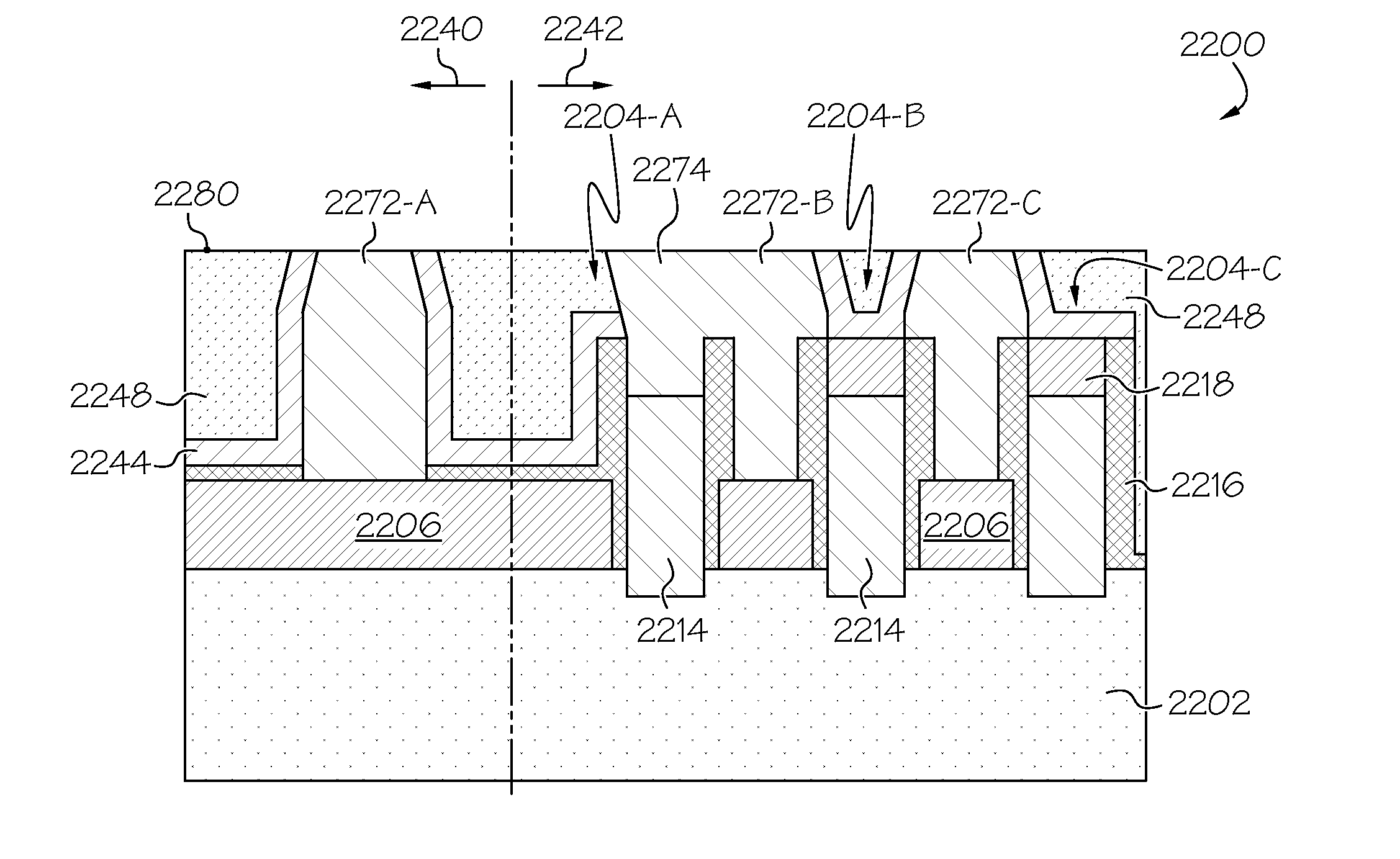
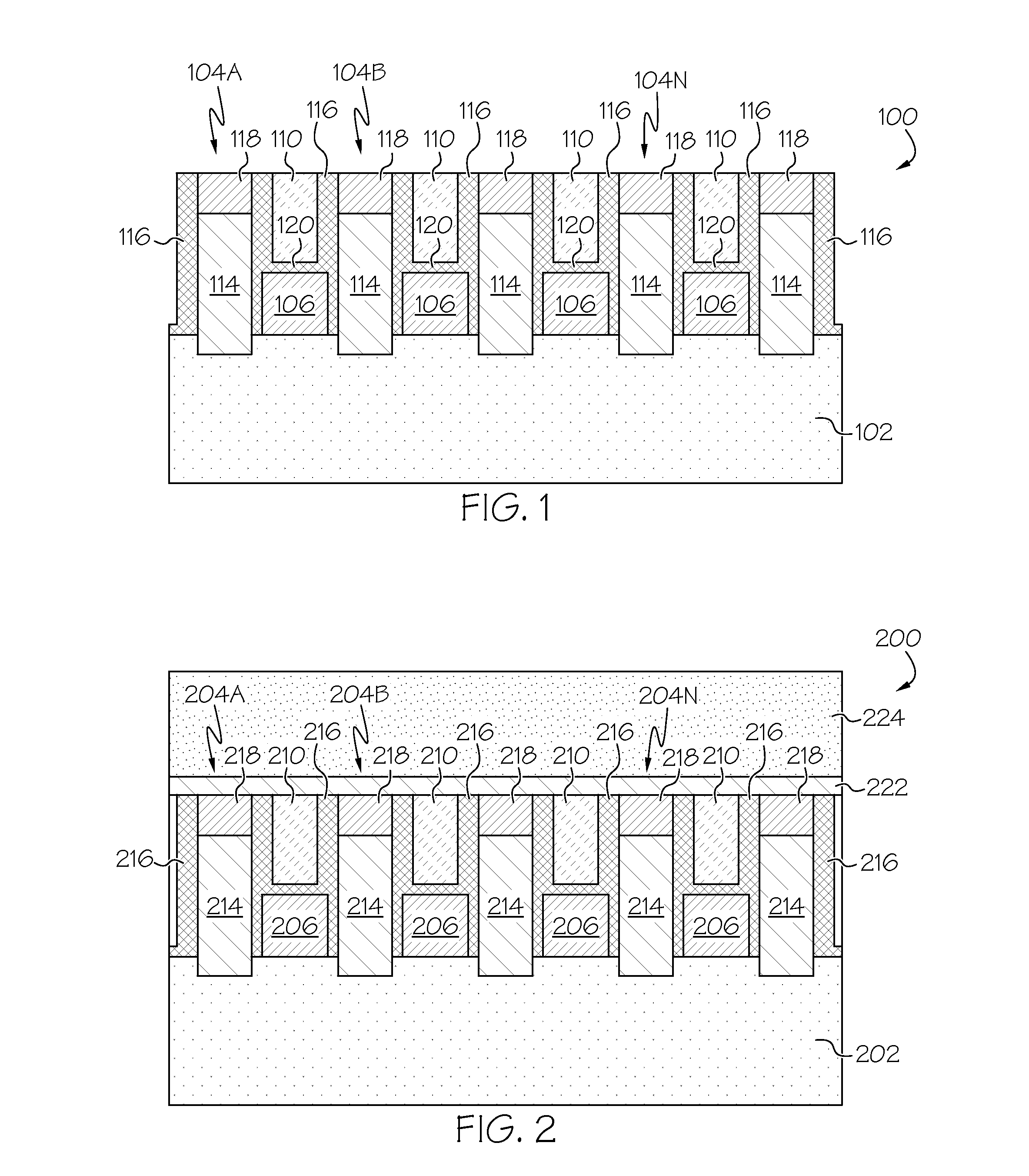
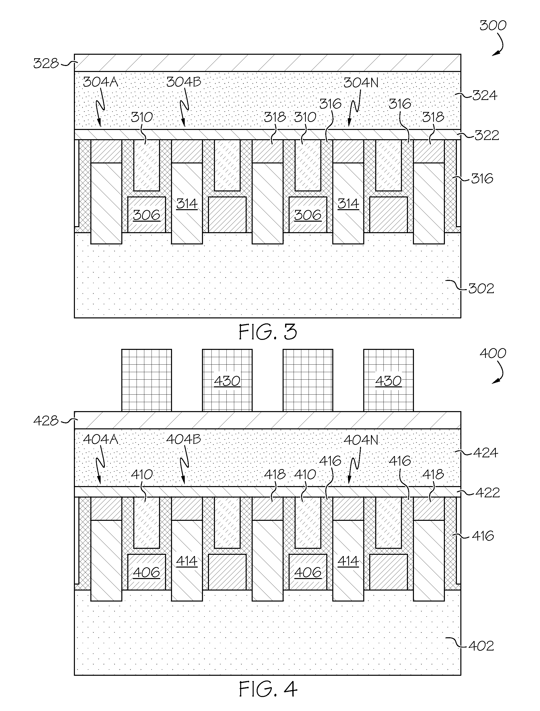
[0047]Exemplary embodiments will now be described more fully herein with reference to the accompanying drawings, in which one or more approaches are shown. It will be appreciated that thi...


PUM


Abstract

Provided are approaches for forming gate and source/drain (S/D) contacts. Specifically, a gate contact opening is formed over at least one of a set of gate structures, a set of S/D contact openings is formed over fins of the semiconductor device, and a metal material is deposited over the semiconductor device to form a gate contact within the gate contact opening and a set of S/D contacts within the set of S/D contact openings. In one approach, nitride remains between the gate contact and at least one of the S/D contacts. In another approach, the device includes merged gate and S/D contacts. This approach provides selective etching to partition areas where oxide will be further removed selectively to nitride to create cavities to metallize and create contact to the S/D, while isolation areas between contact areas are enclosed in nitride and do not get removed during the oxide etch.

Description

BACKGROUND[0001]1. Technical Field[0002]This invention relates generally to the field of semiconductors, and more particularly, to approaches used in forming contacts in semiconductor devices.[0003]2. Related Art[0004]A typical integrated circuit (IC) chip includes a stack of several levels or sequentially formed layers of shapes. Each layer is stacked or overlaid on a prior layer and patterned to form the shapes that define devices (e.g., fin-type field effect transistors (FinFETs)) and connect the devices into circuits. In a typical state of the art complementary insulated gate FinFET process, such as what is normally referred to as CMOS, layers are formed on a wafer to form the devices on a surface of the wafer. Further, the surface may be the surface of a silicon layer on a silicon on insulator (SOI) wafer. A simple FinFET is formed by the intersection of two shapes, i.e., a gate layer rectangle on a silicon island formed from the silicon surface layer. Each of these layers of s...

Claims


Application Information

Patent Timeline
IPC IPC(8): H01L21/28H01L29/417H01L21/283
CPCH01L21/28008H01L29/41775H01L21/283H01L21/76895H01L21/76897H01L21/76804H01L21/76831H01L29/41791H01L29/66795H01L29/785
Inventor BOUCHE, GUILLAUMEWEI, ANDY CHIH-HUNGWELLS, GABRIEL PADRONLABONTE, ANDRE P.WAN, JING
Owner GLOBALFOUNDRIES INC
Why Eureka
Try Eureka