Imprinted Memory

a memory and imprinting technology, applied in the field of integrated circuits, can solve the problems of difficult application of ret techniques to data masks, increase the data volume of sub-100 nm masks, and increase the complexity of manufacturing, so as to achieve easy nanometer printing, reduce data recording costs, and avoid complex mask manufacturing processes

Inactive Publication Date: 2015-11-05
ZHANG GUOBIAO
View PDF9 Cites 0 Cited by
  • Summary
  • Abstract
  • Description
  • Claims
  • Application Information

AI Technical Summary

Benefits of technology

[0008]It is a principle object of the present invention to provide a method to lower the data-recording cost for the sub-100 nm printed memory.
[0009]It is a further object of the present invention to provide an economical sub-100 nm printed memory.
[0010]In accordance with these and other objects of the present invention, an imprinted memory, more particularly a three-dimensional imprinted memory (3D-iP), is disclosed.
[0011]The present invention discloses an imprinted memory, more particularly a three-dimensional imprinted memory (3D-iP). It uses imprint-lithography to record data. Imprint-lithography is also referred to as nano-imprint lithography (NIL). It creates patterns by mechanical deformation of imprint resist and subsequent processes. A key benefit of using imprint-lithography for data-recording is the low-cost of its data-template. Here, the data-template is the template (also referred to as stamp, master or mold) that is used to transfer data-pattern to the data-coding layer. Because the pattern on the data-template is a 1:1 copy of the pattern in the data-coding layer, i.e. there is no optical distortion, the data-template doses not need OPC and therefore, the data volume for a data-template is much less than that for a data-mask. In addition, because imprint-lithography does not suffer from optical diffraction, the data-template does not need to use phase-shift technique. Hence, complex mask manufacturing process can be avoided. More importantly, imprint-lithography can easily print the nanometer-scale non-periodic pattern (i.e., the data-pattern exhibits no nanometer-scale periodicity). Overall, for the sub-100 nm nodes, the data-template is much less expensive that the data-mask. As a result, the imprinted memory, which uses imprint-lithography to record data, has a low data-recording cost than the mask-ROM, which uses photo-lithography to record data.

Problems solved by technology

The introduction of these RET techniques greatly increases the data volume for the sub-100 nm mask, as well as its manufacturing complexity.
On the other hand, because the data-pattern exhibits no nanometer-scale periodicity, it is difficult to apply the RET techniques to the data-mask.
This significantly increases the manufacturing complexity as well as the cost of the data-mask.
The rising data-mask cost makes mask-ROM economically un-viable below 100 nm.

Method used


Image

  • Imprinted Memory
  • Imprinted Memory
  • Imprinted Memory

Examples


Embodiment Construction

[0017]Those of ordinary skills in the art will realize that the following description of the present invention is illustrative only and is not intended to be in any way limiting. Other embodiments of the invention will readily suggest themselves to such skilled persons from an examination of the within disclosure.

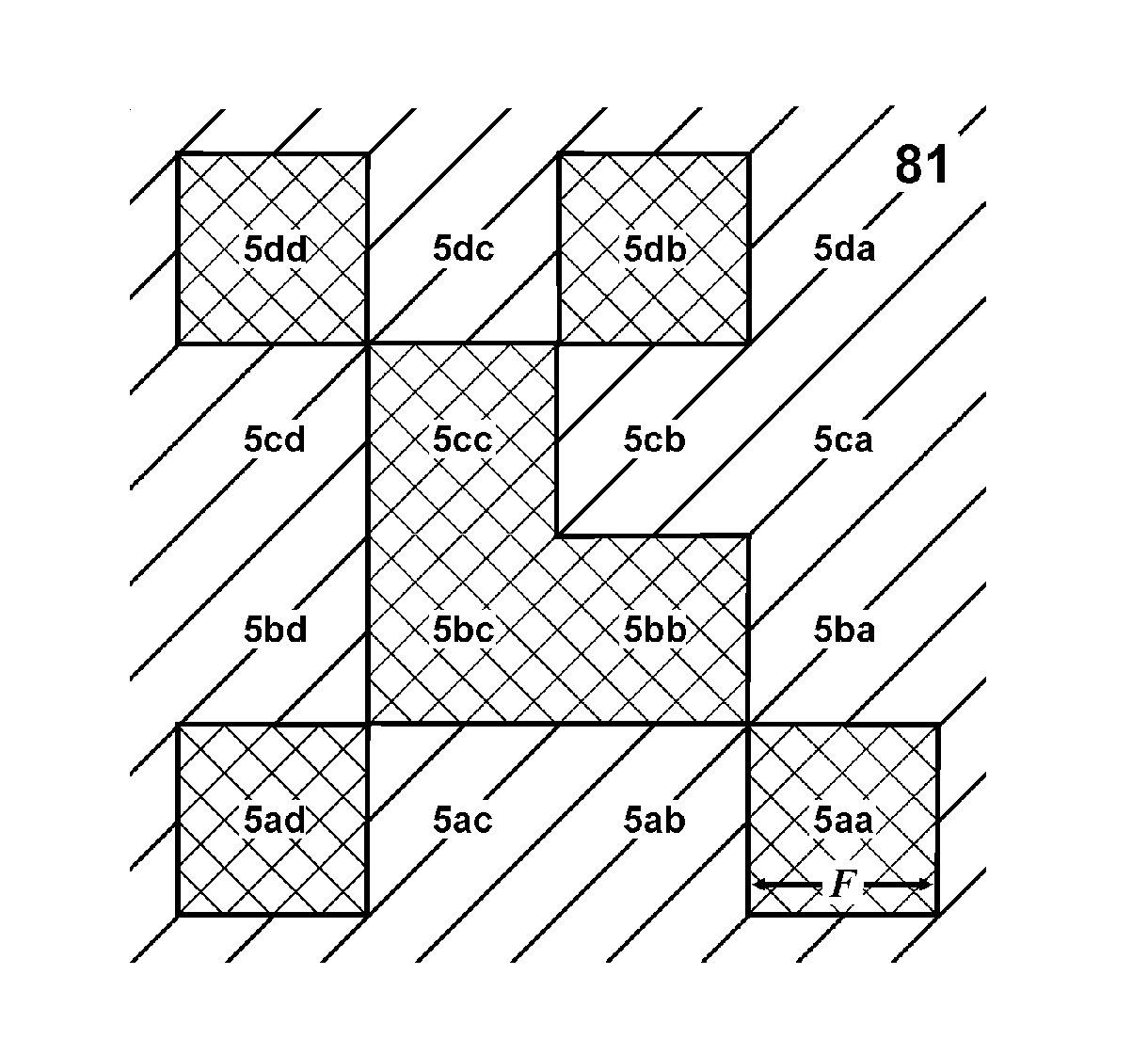
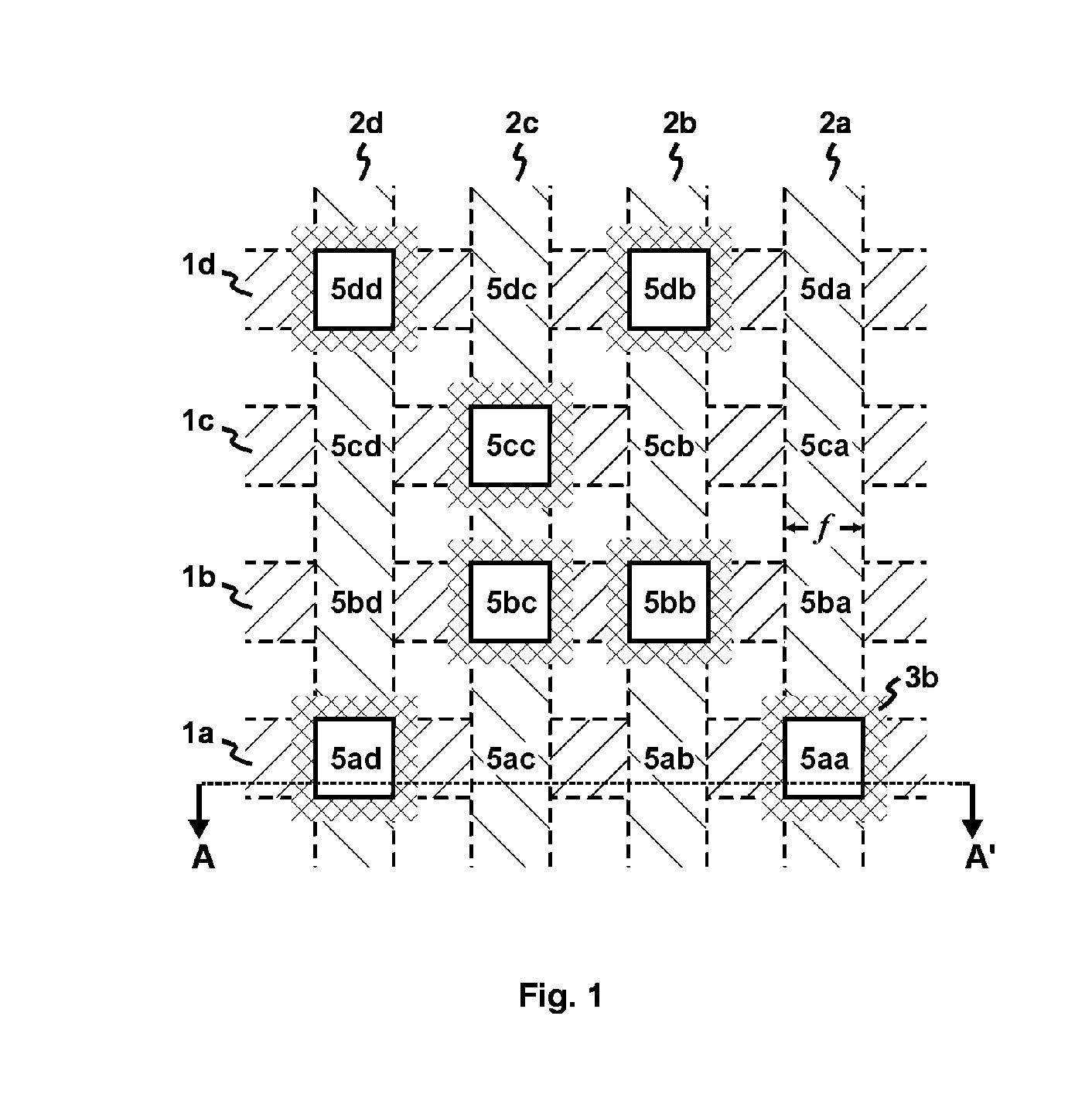
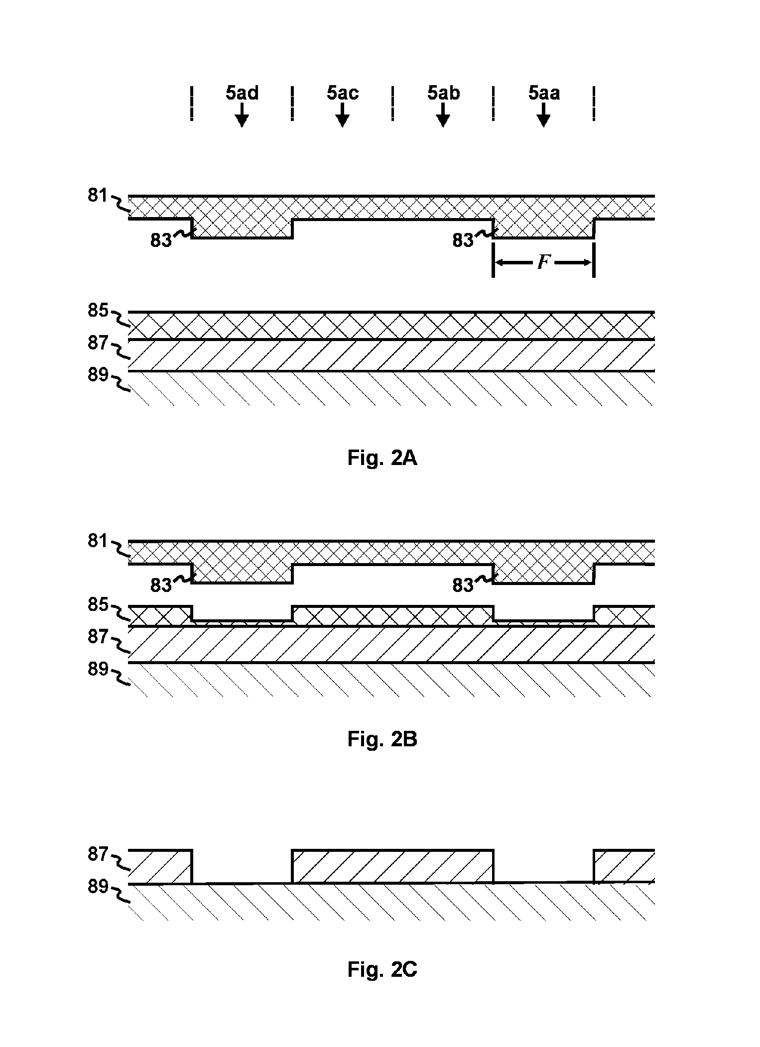
[0018]To lower the data-recording cost, the present invention discloses an imprinted memory, more particularly a three-dimensional imprinted memory (3D-iP). As to its final physical structures, the imprinted memory is same as the mask-ROM. Both use the data-pattern in the data-coding layer to store data. They differ in their data-recording method: the imprinted memory uses imprint-lithography, while the mask-ROM uses photo-lithography. These methods have different data-recording cost: the data-template used by imprint-lithography is much less expensive than the data-mask used by photo-lithography.

[0019]Imprint-lithography creates patterns by mechanical deformation of imprin...


PUM


Abstract

The present invention discloses an imprinted memory, more particularly a three-dimensional imprinted memory (3D-iP). Instead of photo-lithography, it uses imprint-lithography (also referred to as nano-imprint lithography, or NIL) to record data. For the sub-100 nm nodes, the data-template used by imprint-lithography is much less expensive than the data-mask used by photo-lithography.

Description

CROSS-REFERENCE TO RELATED APPLICATIONS[0001]This is a continuation-in-part of application “Imprinted Memory”, application Ser. No. 13 / 602,095, filed Aug. 31, 2012, which claims benefit of a provisional application “Three-Dimensional Printed Memory”, Application Ser. No. 61 / 529,919, filed Sep. 1, 2011.BACKGROUND[0002]1. Technical Field of the Invention[0003]The present invention relates to the field of integrated circuit, and more particularly to printed memory.[0004]2. Prior Arts[0005]Printed memory comprises at least a data-coding layer whose pattern is printed in factory. This pattern, referred to as data-pattern, represents the digital data stored in the printed memory (referring to U.S. patent application “Three-Dimensional Printed Memory”, Ser. No. 13 / 570,216, filed Aug. 8, 2012). A common printed memory is mask-programmed read-only memory (mask-ROM), whose data-printing method is photo-lithography. As illustrated in FIG. 1, this mask-ROM comprises a plurality of top address l...

Claims


Application Information

Patent Timeline
Patent Type & Authority Applications(United States)
IPC IPC(8): H01L45/00H01L27/24
CPCH01L45/1666H01L45/122H01L27/2481H01L45/1608H01L27/1021G03F7/0002H01L21/32139H10B20/38H10B20/50H10B63/84H10N70/061H10N70/021H10N70/821
Inventor ZHANG, GUOBIAO
Owner ZHANG GUOBIAO
Why Eureka
Try Eureka