Supercharge Your Innovation With Domain-Expert AI Agents!

Cascoded high voltage junction field effect transistor

a high-voltage junction field effect transistor and cascode technology, applied in the field of cascoded high-voltage junction field-effect transistors, can solve the problems of weaker jfet devices, unacceptably large vp variations, limited process for manufacturing the conventional high-voltage junction field-effect transistor devices, etc., and achieve low pinch off voltage and low pinch off voltage variations.

Active Publication Date: 2015-11-19
ALPHA & OMEGA SEMICON INC
View PDF1 Cites 9 Cited by
  • Summary
  • Abstract
  • Description
  • Claims
  • Application Information

AI Technical Summary

Benefits of technology

The present invention provides a new and improved device configuration and manufacturing method for a cascoded JFET device. It includes a low voltage JFET with a source region connected to a shallow buried channel region below a top gate, and a high voltage JFET device is formed on the drain of the low voltage JFET. This device configuration has the benefit of a high pinch off voltage as an operational characteristic of the high voltage JFET device, with a low variation in VP as an operational characteristic of the low voltage JFET. This two-stage cascoded JFET device achieves improved performance by combining the advantages of both high and low voltage JFETs.

Problems solved by technology

The processes for manufacturing the conventional high voltage junction field effect transistor (JFET) device is limited by the highly sensitive performance variations caused by the thickness variations of the epitaxial layer functioning as the channel region.
Such Vp variations may be unacceptably large, especially when deep submicron technologies are implemented.
But if the pinch off voltage Vp has large variations, the target pinch off voltage Vp must also be reduced accordingly to ensure that it does not exceed the maximum allowed voltage, resulting in a weaker JFET device.
A JFET with a low Vp typically has a large channel resistance and cannot handle much current for its given size.
The size and production costs of such JFET devices are therefore increased.
However, a JFET with shallow channel and gate region implant has a low operating voltage.
For higher voltage operations, there are still limitations and difficulties for JFET devices manufactured with the conventional processes and configurations due to the thickness variations of the epitaxial layer and the sensitivities of the pinch off voltage (Vp) variations caused by these thickness variations.

Method used


Image

  • Cascoded high voltage junction field effect transistor
  • Cascoded high voltage junction field effect transistor
  • Cascoded high voltage junction field effect transistor

Examples


Embodiment Construction

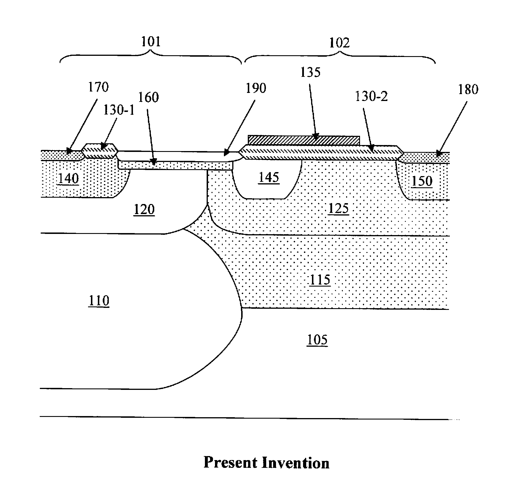
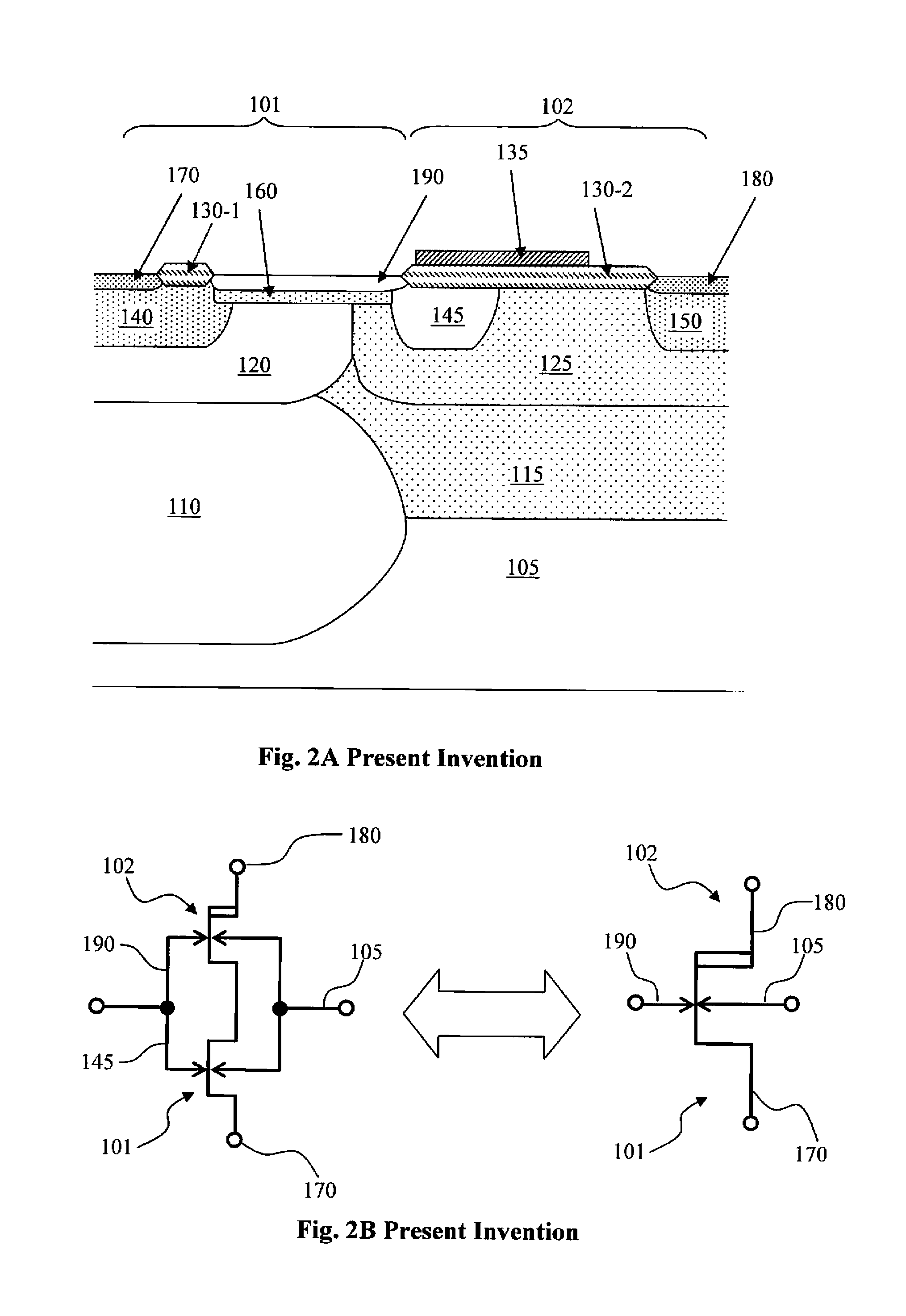
[0024]FIG. 2A is a cross sectional view of a cascoded high voltage junction field effect transistor (JFET) device of this invention. The cascoded HV JFET device is formed with a low voltage JFET 101 on the left cascoded to a high voltage JFET 102 on the right. The low voltage JFET 101 is formed in a high voltage P-well (HVPW) 120 on top of a P-buried layer (PBL) 110 supported on a (P-type) semiconductor substrate 105, and has an N+ source region 170 near the top surface of an N-well 140 encompassed in the HVPW 120. A high voltage well is a region having low doping and deep junction depth, which can sustain high voltage. The low voltage JFET 101 further includes a shallow N-channel 160 disposed immediately below a P+ top gate region 190. The shallow N-channel 160 is formed with a light dosage and semi-high energy implant in the lightly doped HVPW 120 and the top gate 190 is formed with a shallow P+ implant. By way of example, the P+ top gate 190 is only 0.1˜0.3 microns deep. The N ch...


PUM


Abstract

A cascoded junction field transistor (JFET) device comprises a first stage high voltage JFET cascoded to a second stage low voltage JFET wherein one of the first and second stages JFET is connected to a drain electrode of another JFET stage.

Description

[0001]This Application is a Continuation Patent Application (CPA) and claim the Priority Date of of a co-pending patent application Ser. No. 13 / 350,074 filed on Jan. 14, 2012 by common inventors of this Application. application Ser. No. 13 / 350,740 is a Continuation Patent Application (CPA) and claim the Priority Date of another patent application Ser. No. 12 / 928,207 filed on Dec. 5, 2010 by common inventors of this Application and now issued into U.S. Pat. No. 8,097,905. The disclosures made in application Ser. Nos. 13 / 350,740 and 12 / 928,107 are hereby incorporated by reference in this Non-provisional Patent Application.BACKGROUND OF THE INVENTION[0002]1. Field of the Invention[0003]The invention relates generally to semiconductor devices. More particularly, this invention relates to configurations and methods to manufacture a cascoded junction field effect transistor (JFET) device including a high voltage and a low voltage JFET to achieve wide operating voltage capability with tigh...

Claims


Application Information

Patent Timeline
IPC IPC(8): H01L29/66
CPCH01L29/66893H01L29/402H01L29/66901H01L21/76264H01L29/0692H01L29/1058H01L29/1066H01L29/808
Inventor TSUCHIKO, HIDEAKI
Owner ALPHA & OMEGA SEMICON INC
Features
  • R&D
  • Intellectual Property
  • Life Sciences
  • Materials
  • Tech Scout
  • Unparalleled Data Quality
  • Higher Quality Content
  • 60% Fewer Hallucinations
Learn More