Memory compression method of electronic device and apparatus thereof

a technology of electronic devices and memory, applied in the direction of instruments, input/output to record carriers, computing, etc., can solve the problems of increasing the size of the system memory used in the electronic device, increasing the complexity of applications, and increasing the size of the system memory, so as to reduce manufacturing costs, reduce manufacturing costs, and effectively secure the available memory space

Active Publication Date: 2015-11-26
SAMSUNG ELECTRONICS CO LTD
View PDF10 Cites 28 Cited by
  • Summary
  • Abstract
  • Description
  • Claims
  • Application Information

AI Technical Summary

Benefits of technology

[0016]According to an embodiment of the present invention, the data corresponding to one or more applications loaded in the memory is selectively compressed, so the available memory space can be effectively secured. Accordingly, the existing memory can be efficiently utilized without adopting an additional memory, so the electronic device can be manufactured at a low cost by reducing the manufacturing cost. In addition, the disk of which the access speed is slow is ruled out to thereby improve the data loading speed.
[0017]In addition, according to an embodiment of the present invention, the memory compression method may be changed depending on system demands to thereby effectively perform the memory compression.
[0018]In addition, according to an embodiment of the present invention, the compression performance can be enhanced by improving a service rate and a compression ratio.

Problems solved by technology

Recently, memory size has increased according to an increase in the complexity of applications.
Although the size of a system memory used in an electronic device has increased according to the trend above, it is not sufficient enough to meet the demands for the memory size required by the applications.
In performing the swapping, the access speed to the disk is normally slower than the access speed to the memory, so the system performance may deteriorate.
However, the memory compression according to the prior art has a trade-off between a service rate and a compression ratio.

Method used


Image

  • Memory compression method of electronic device and apparatus thereof
  • Memory compression method of electronic device and apparatus thereof
  • Memory compression method of electronic device and apparatus thereof

Examples


Embodiment Construction

[0039]Hereinafter, various embodiments of the present invention will be described in detail with reference to the accompanying drawings. It should be noted that the same elements will be designated by the same reference numerals although they are shown in different drawings. Further, a detailed description of a known function and configuration which may make the subject matter of the present invention unclear will be omitted. Hereinafter, it should be noted that only the descriptions will be provided that may help understanding the operations provided in association with the various embodiments of the present invention, and other descriptions will be omitted to avoid making the subject matter of the present invention rather unclear.

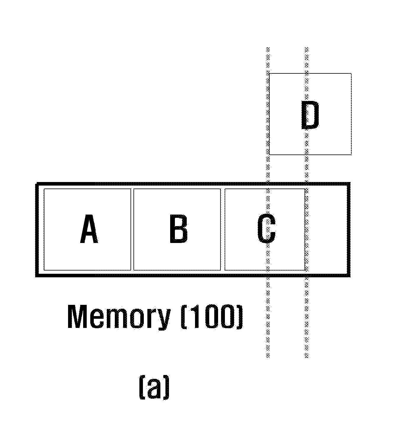
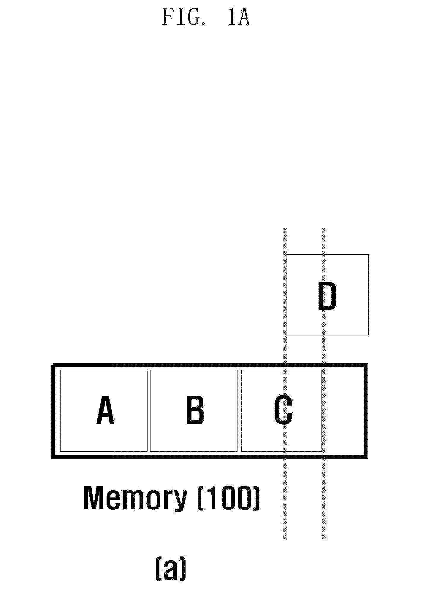
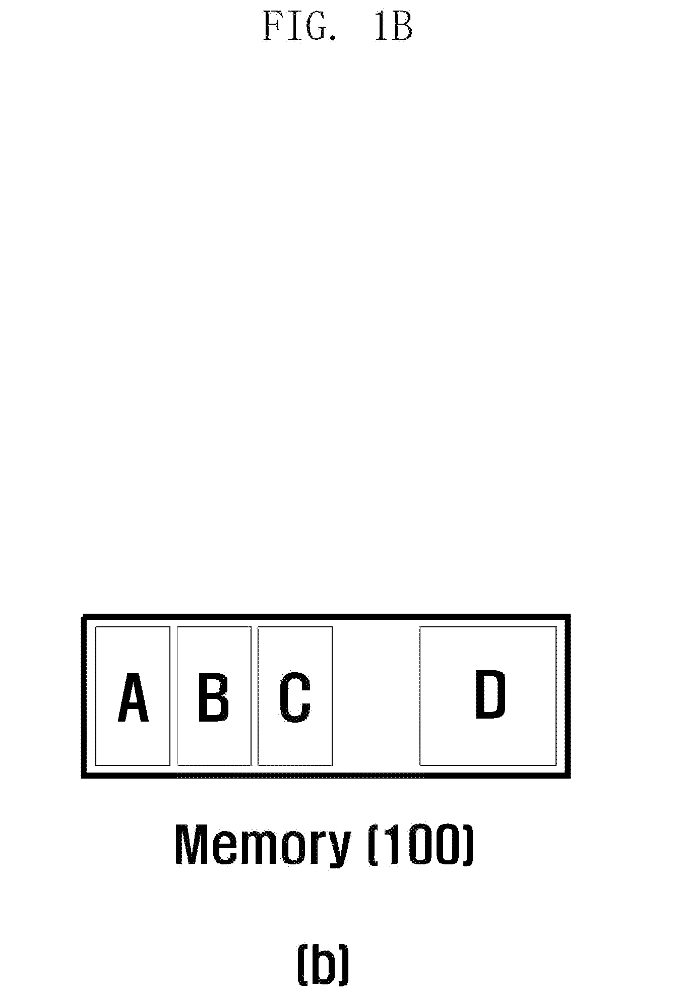
[0040]FIG. 1 illustrates a memory compression procedure according to an embodiment of the present invention.

[0041]FIG. 1a shows that the electronic device status has been changed while at least one application is loaded in a memory 100. The electronic dev...


PUM


Abstract

Disclosed are a memory compression method of an electronic device and an apparatus thereof. The method for compressing memory in an electronic device may include: detecting a request for executing the first application; determining whether or not the memory compression is required for the execution of the first application; when the memory compression is required, compressing the memory corresponding to an application in progress in the background of the electronic device; and executing the first application.

Description

TECHNICAL FIELD[0001]This application claims priority under 35 U.S.C. §119(a) to Korean Application Serial Nos. 10-2013-0124885 & 10-2013-0128848, which were filed in the Korean Intellectual Property Office on Oct. 18, 2013 & Oct. 28, 2013, the entire content of which is hereby incorporated by reference.BACKGROUND ART[0002]The present invention relates generally to an electronic device, and more particularly, to a memory compression method of an electronic device and an apparatus thereof.[0003]Recently, memory size has increased according to an increase in the complexity of applications. Although the size of a system memory used in an electronic device has increased according to the trend above, it is not sufficient enough to meet the demands for the memory size required by the applications.[0004]One of the methods for securing an available memory space is swapping. The swapping refers to a method by which data is transferred from the memory space to the disk space in order to secur...

Claims


Application Information

Patent Timeline
Patent Type & Authority Applications(United States)
IPC IPC(8): G06F3/06
CPCG06F3/0608G06F3/0673G06F3/0659G06F3/064G06F12/023G06F2212/401G06F3/0625G06F3/0634G06F3/0656G06F3/0638G06F12/00G06F3/061
Inventor KANG, BYOUNGIKPARK, JINYOUNGSHIN, HEESUBLEE, SEUNGWOOK
Owner SAMSUNG ELECTRONICS CO LTD
Why Eureka
Try Eureka