Switching element and method for fabricating semiconductor switching device

a switching device and switching element technology, applied in semiconductor devices, digital storage, instruments, etc., can solve the problems of embedded memories, unsuitable for being embedded in logic lsi, and loss of stored information of edrams, so as to prevent false writes and false operations, the effect of improving reliability

Active Publication Date: 2015-11-26
NANOBRIDGE SEMICON INC
View PDF13 Cites 21 Cited by
  • Summary
  • Abstract
  • Description
  • Claims
  • Application Information

AI Technical Summary

Benefits of technology

[0056]A switching element of the present invention is capable of preventing false writes and false operations of variable resistance elements and improving the reliability.

Problems solved by technology

The eDRAM loses stored information when power is removed from it.
Accordingly, embedded memories have problems, including the problem that they are unsuitable for being embedded in a logic LSI (Large Scale Integrated circuit) which operates at a low voltage (1 V or lower).

Method used


Image

  • Switching element and method for fabricating semiconductor switching device
  • Switching element and method for fabricating semiconductor switching device
  • Switching element and method for fabricating semiconductor switching device

Examples


first exemplary embodiment

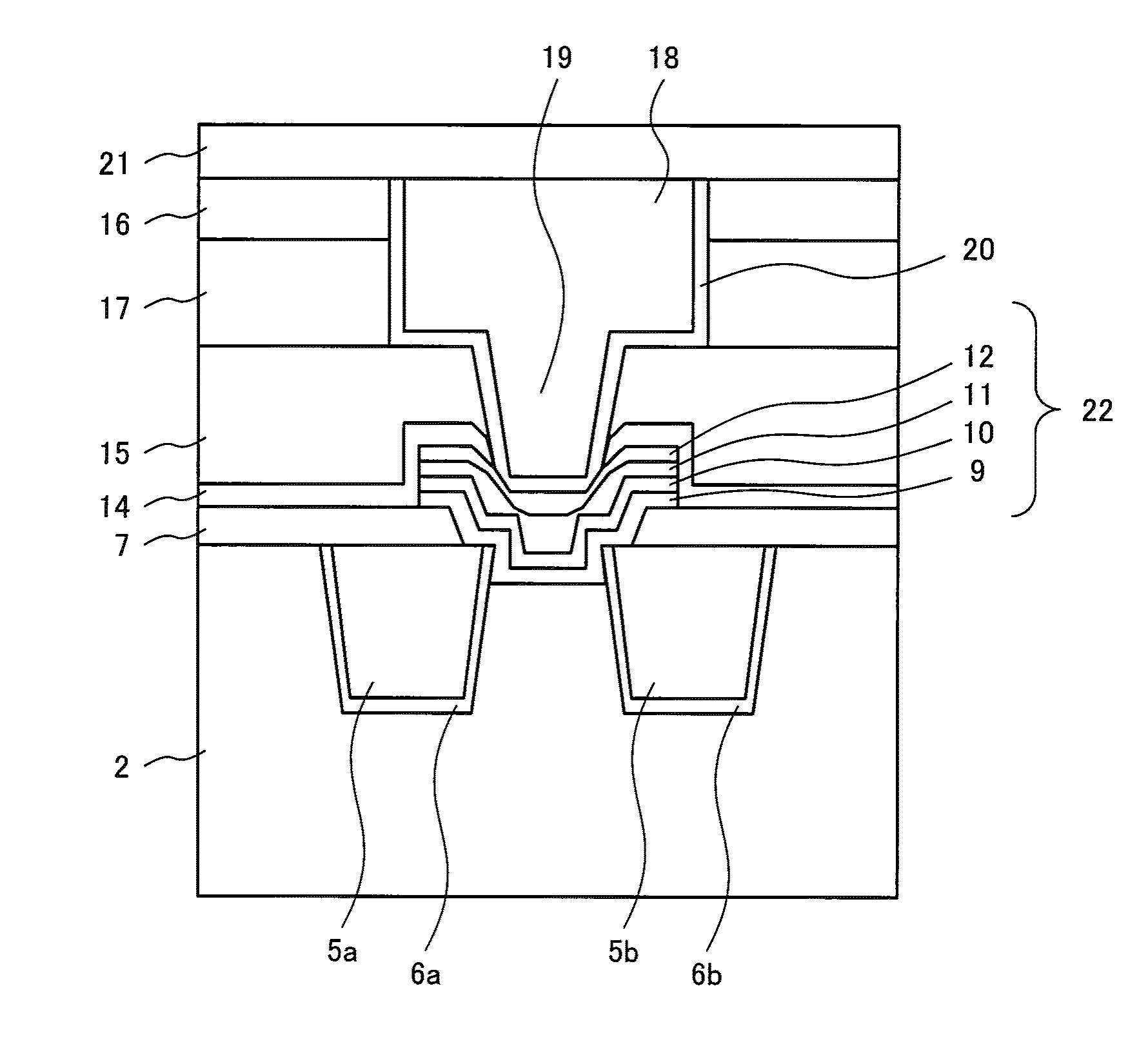
[0120]As illustrated in FIG. 3, in a switching element, a first variable resistance element 101 includes a first electrode 101a, a first variable resistance film 101b and a second electrode 101c, and a second variable resistance element 102 includes a first electrode 102a, a second variable resistance film 102b and a second electrode 102c. A rectifier 103 includes a first electrode 103a, a rectifying film 103b and a second electrode 103c.

[0121]Each of the first electrodes 101a, 102a includes an active electrode which supplies metallic ions. The variable resistance films 101a, 102b include a solid electrolyte layer which conducts ionized metal. Each of the second electrodes 101c, 102c includes an inactive electrode that does not react with the metallic ions.

[0122]The rectifying film 103b may be a film such as Poole-Frenkel insulating film, a Schottky insulating film, or a threshold-switching volatile variable resistance film.

[0123]Next, a factor that minimizes false writes and false...

second exemplary embodiment

[0128]FIG. 4 illustrates a device structure in which inactive electrodes are interconnected. The device structure includes two bipolar solid electrolyte switches, and solid electrolytes 402 of variable resistance elements described above are interconnected each other, inactive electrodes 403 of the variable resistance elements are interconnected each other, rectifying elements 404 are interconnected each other, control electrodes (third electrodes) 405 are interconnected each other. Signals are input and output through two first electrodes (a first active electrode 401a, a second active electrode 401b) that are not interconnected.

[0129]To place the switching element in the on state (low-resistance state), a voltage is applied to the control electrode (third electrode) 405 to form metal bridges 406a, 406b from the first active electrode 401a and the second active electrode 401b, respectively, in the solid electrolyte 402. As a result, the first active electrode 401, the inactive elec...

third exemplary embodiment

[0131]A third exemplary embodiment of the present invention will be described next. In the third exemplary embodiment, variable resistance elements (of the first exemplary embodiment) each including a control electrode (third electrode) are arranged in an array and used as a switch (crossbar switch), thereby the switch element area can be reduced.

[0132]FIG. 5 is a diagram illustrating a configuration of the third exemplary embodiment. A configuration in which variable resistance elements are arranged in an array to form a crossbar switch is illustrated in FIG. 5 as an equivalent circuit.

[0133]Complementary variable resistance elements achieve an improved reliability against disturbance when the complementary variable resistance elements are place in the off state, because: (1) voltage is divided between two variable resistance elements and (2) bipolar variable resistance elements are connected in series in different set voltage directions, as illustrated in FIG. 5. Furthermore, the ...


PUM


Abstract

In switching elements each using a two-terminal-type variable resistance element, improper writing or any improper operation is often caused and the reliability of the switching elements cannot be improved easily. A switching element according to the present invention is equipped with a first variable resistance element equipped with a first input / output terminal and a first connection terminal, a second variable resistance element equipped with a second input / output terminal and a second connection terminal, and a rectifying element equipped with a control terminal and a third connection terminal, wherein the first connection terminal, the second connection terminal and the third connection terminal are connected to one another.

Description

TECHNICAL FIELD[0001]The present invention relates to a switching element and a method for fabricating a semiconductor switching device and, in particular, to a switching element including a nonvolatile variable resistance element and a method for fabricating a semiconductor switching device including a nonvolatile variable resistance element.BACKGROUND ART[0002]Semiconductor devices (in particular, silicon devices) have been increased in the scale of integration and fourfold in every three years by miniaturization (a scaling law called Moore's Law) and reduced in power consumption. In recent years, the gate lengths of MOSFETs (Metal Oxide Semiconductor Field Effect Transistors) are 20 nm or less. Because of rising costs for lithography processes (equipment prices and mask set prices) and the physical limits of device scaling (operating limits and the variation limits), there has been need for improvement in the performance of highly integrated devices through an approach other than...

Claims


Application Information

Patent Timeline
Patent Type & Authority Applications(United States)
IPC IPC(8): H01L45/00H01L27/24
CPCH01L45/126H01L45/1683H01L27/2436H01L45/1233G11C13/0002G11C2213/15G11C2213/78H10B63/20H10B63/82H10N70/20H10N70/245H10N70/826H10N70/8416H10N70/8833H10N70/063H10B63/22H10B63/30H10B63/24H10N70/8413H10N70/066H10N70/231H10N70/8418
Inventor TADA, MUNEHIROSAKAMOTO, TOSHITSUGUBANNO, NAOKIOKAMOTO, KOICHIRO
Owner NANOBRIDGE SEMICON INC
Why Eureka
Try Eureka