Semiconductor device for preventing erroneous write to memory cell in switching operational mode between normal mode and standby mode

a technology of memory cell and write device, which is applied in the direction of information storage, static storage, digital storage, etc., can solve the problems of conventional techniques described above cannot prevent erroneous write to the memory cell

Active Publication Date: 2009-08-06
RENESAS ELECTRONICS CORP
View PDF4 Cites 20 Cited by
  • Summary
  • Abstract
  • Description
  • Claims
  • Application Information

AI Technical Summary

Benefits of technology

[0012]According to the present invention, before the supply of the second power supply voltage is halted, a voltage of each of the plurality of word lines is preliminarily clamped to the reference voltage, and thereby the power supply line of the word line drivers is interrupted. Further, after the supply of the second power supply voltage is started, voltage clamp of the word line drivers is cancelled, and the power supply line of the word line drivers is connected. Therefore, the major advantage of the present invention is to be able to prevent erroneous write to the memory cell by preventing a noise, which is generated by switching between the normal mode and the standby mode, from flowing to the word lines.

Problems solved by technology

When an operational mode of the semiconductor device is shifted from a normal mode to a standby mode, or returns to the normal mode from the standby mode, a noise may be generated in association with a falling edge or a rising edge of the power supply voltage.
When the generated noise flows from the word line driver to the word line, an access transistor of the memory cell may be brought into conduction to cause erroneous write to the memory cell.
The conventional techniques described above cannot sufficiently prevent the erroneous write to the memory cell, caused by such a noise.

Method used


Image

  • Semiconductor device for preventing erroneous write to memory cell in switching operational mode between normal mode and standby mode
  • Semiconductor device for preventing erroneous write to memory cell in switching operational mode between normal mode and standby mode
  • Semiconductor device for preventing erroneous write to memory cell in switching operational mode between normal mode and standby mode

Examples


first embodiment

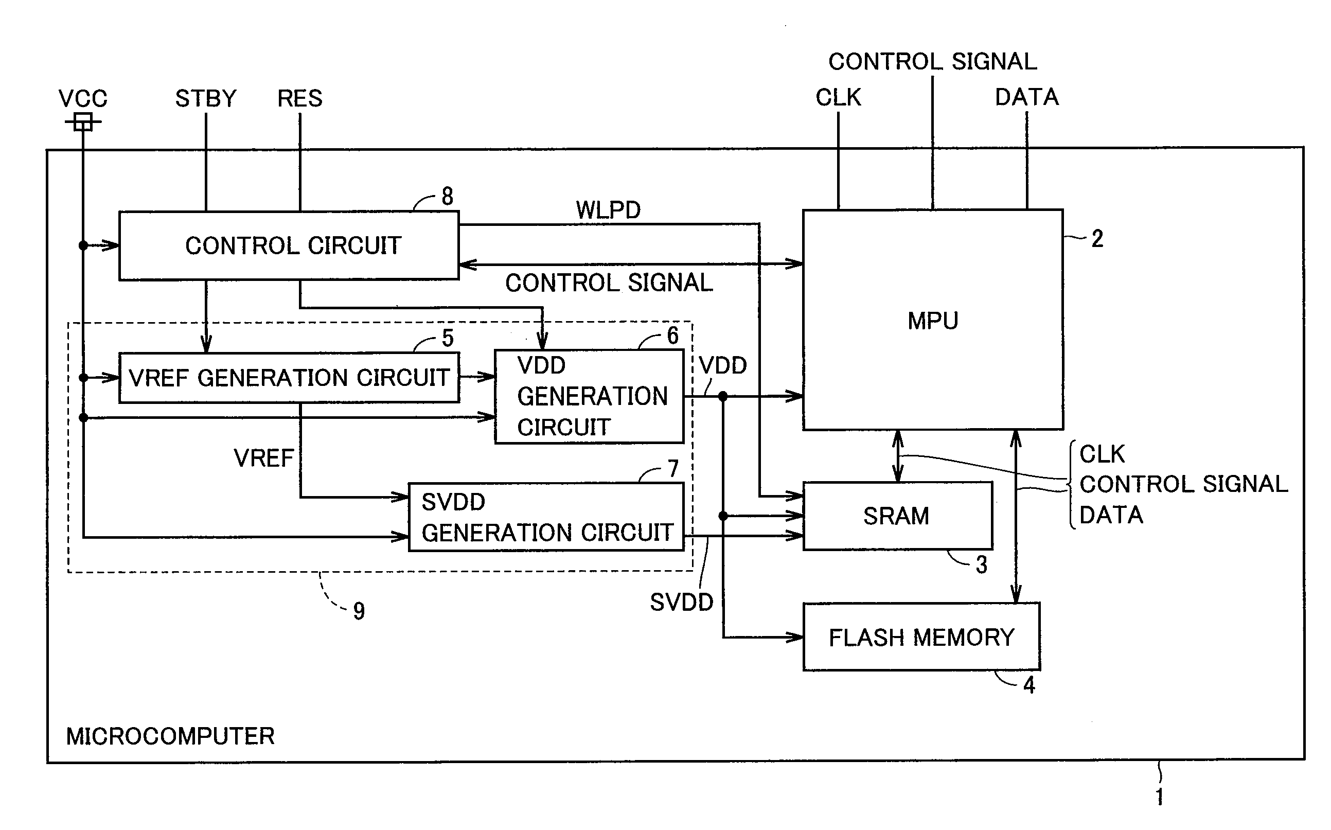
[0025]FIG. 1 is a block diagram that shows a configuration of a semiconductor device 1 in a first embodiment of the present invention. FIG. 1 shows a microcomputer as an example of semiconductor device 1.

[0026]With reference to FIG. 1, semiconductor device 1 includes a microprocessor unit (MPU) 2, an SRAM 3, a flash memory 4, a VREF generation circuit 5, a VDD generation circuit 6, an SVDD generation circuit 7, and a control circuit 8. VREF generation circuit 5, VDD generation circuit 6, and SVDD generation circuit 7 configure a power supply unit 9.

[0027]Semiconductor device 1 switches an operational mode between a normal mode and a standby mode in accordance with a standby signal STBY and a reset signal RES which are supplied from an outside. In the standby mode in which both of standby signal STBY and reset signal RES are at an L level, power supply to the circuits other than some circuits necessary for holding data is halted to reduce power consumption.

[0028]Specifically, VREF ge...

second embodiment

[0106]In a second embodiment, there is shown a method of preventing erroneous write of data in the standby mode, by utilizing control signal WLPD outputted from control circuit 8 in FIG. 1, and by using means different from the means in the first embodiment. The method in the second embodiment may be implemented in combination with the first embodiment, or may be implemented independently of the first embodiment.

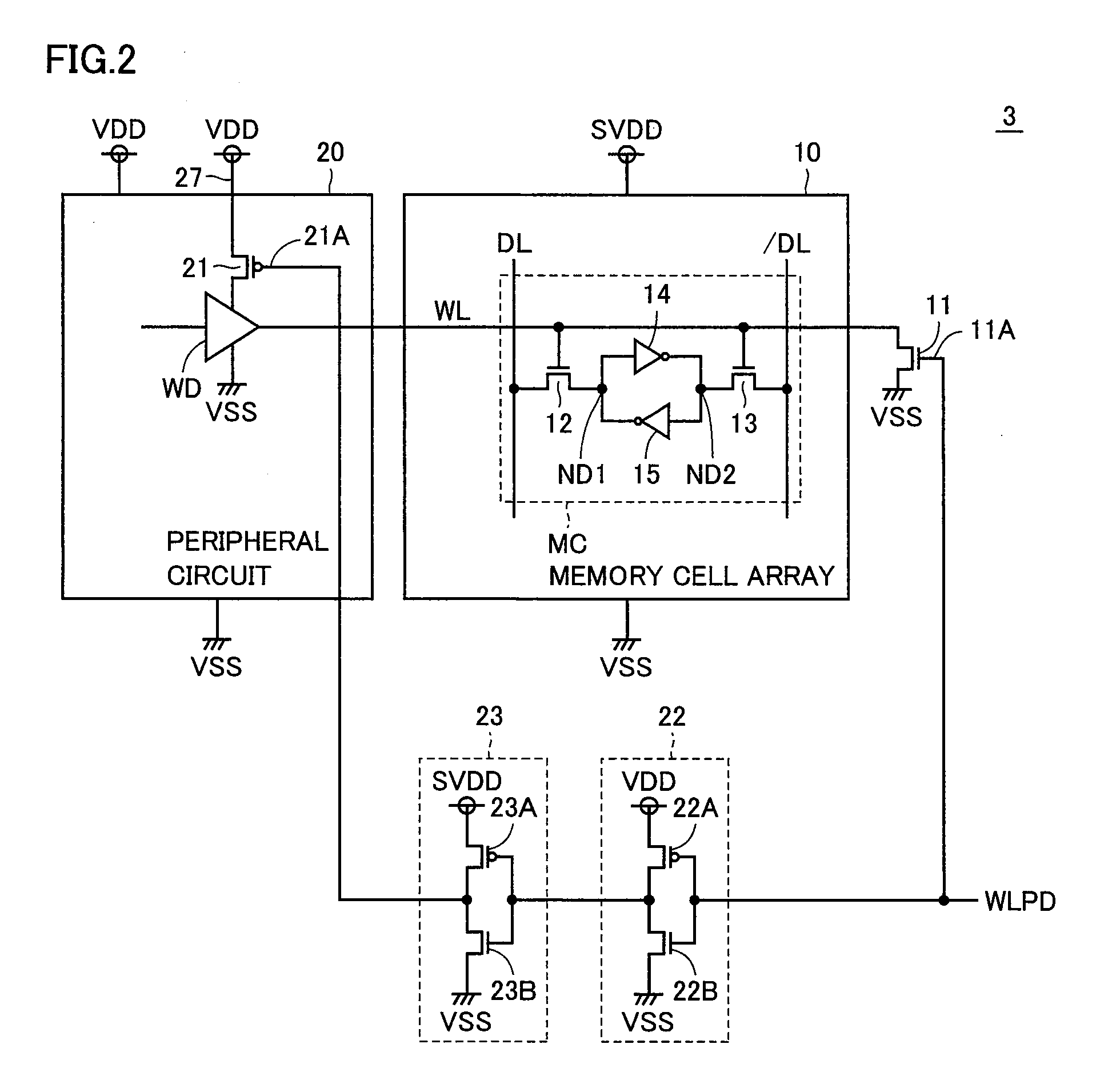
[0107]FIG. 10 is a circuit diagram that shows a configuration of an SRAM 3B in the second embodiment of the present invention.

[0108]With reference to FIG. 10, SRAM 3B in the second embodiment differs from SRAM 3 in the first embodiment shown in FIG. 5 in that it further includes a voltage-setting circuit 80 for setting voltages of data line pair DL, / DL to internal power supply voltage VDD, and CMOS inverters 84, 85.

[0109]Voltage-setting circuit 80 includes P-channel MOS transistors 80A, 80B, 80C. Among them, MOS transistors 80A, 80B have sources and back gates to which inte...


PUM


Abstract

When an operational mode is shifted to a standby mode, a first transistor is brought into a conduction state by a control signal, and a word line is thereby clamped to a ground voltage. Further, a second transistor is brought into a non-conduction state, and supply of an internal power supply voltage to a word line driver is shut off. Subsequently, the supply of the internal power supply voltage is halted for saving electrical power. When the operational mode returns to a normal mode, the supply of the internal power supply voltage is started, and subsequently, the first transistor is brought into the non-conduction state by the control signal, and the second transistor is thereby brought into the conduction state.

Description

BACKGROUND OF THE INVENTION[0001]1. Field of the Invention[0002]The present invention relates to a semiconductor device, and particularly relates to a semiconductor device including a static-type semiconductor memory.[0003]2. Description of the Background Art[0004]In a low-power-consumption semiconductor device, a standby mode (sleep mode) in which power supply is shut off may be provided. In the standby mode, a power voltage is supplied only to some circuits necessary for holding data, such as a memory cell of an SRAM (Static Random Access Memory).[0005]In the SRAM described in Japanese Patent Laying-Open No. 11-219589, for example, supply of a power supply voltage to the circuits other than a memory cell and a word line potential clamping circuit is shut off during a sleep period in which data is held. The word line potential clamping circuit clamps the word line to a non-selection level during the sleep period, so as to prevent instability in word line potential and the resultant...

Claims


Application Information

Patent Timeline
Patent Type & Authority Applications(United States)
IPC IPC(8): G11C5/14G11C8/08
CPCG11C5/14G11C5/148G11C11/413G11C8/10G11C11/412G11C8/08G11C11/417
Inventor AGARI, TAKESHISATO, HIROTOSHIAKAI, KIYOYASUSENDA, MINORUNAKAI, HIROAKI
Owner RENESAS ELECTRONICS CORP
Why Eureka
Try Eureka