Interleaved a/d converter

a converter and interleave technology, applied in the field of interleaved a/d converters, can solve the problems of reducing the resolution of the effective resolution, the speed of the single adc that can perform sampling while maintaining an effective resolution in 10 bit or more may be limited to approximately 250 mhz, and the resolution to be guaranteed technique is also limited, so as to prevent the resolution from decreasing.

Active Publication Date: 2015-11-26
HITACHI LTD
View PDF3 Cites 12 Cited by
  • Summary
  • Abstract
  • Description
  • Claims
  • Application Information

AI Technical Summary

Benefits of technology

[0021]According to the invention, the sampling timing of paired ADCs that are likely to be the greatest interference from symmetry of a differential signal is accurately inscribed with a π-phase difference by the common sampling clock. Thus, the interference between ADC inputs due to an error from an ideal value of the ADC sampling timing is suppressed. Furthermore, the input signal is transmitted to the ADC sampling circuit of the subsequent stage by the buffer, but the electric charge released from the ADC sampling circuit is blocked by the buffer and is not transmitted to the common analog input signal line. Other ADCs connected in parallel do not interfere with each other and the characteristics degradation by the insertion of the buffer is suppressed by the digital correction. Thus, it is possible to prevent the resolution from decreasing.

Problems solved by technology

However, a speed of single ADC that can perform sampling while maintaining an effective resolution in 10 bit or more may be limited to approximately 250 MHz from rate-limiting derived from frequency characteristics of a transistor configuring the ADC.
Meanwhile, the technique is also limited in the resolution to be guaranteed due to mismatch such as DC offset of each ADC which is connected in parallel, variation of a conversion gain, and a deviation of sampling clock timing.
However, the mismatch problem is solved and a clue is found in the improvement of the effective resolution while maintaining the high speed of the interleaved ADC, but new problem occurs.
However, each ADC sampling circuit releases an electric charge with respect to an input in a sampling clock edge and another parallel ADC samples the signal disturbed by the electric charge, and thereby a problem that the effective resolution is limited occurs.
Here, it is important that the digital correction scheme cannot be effective against irregular factors and leads to a decrease in the effective resolution.
Since the electric charge released from the input of the ADC irregularly depends on the input signal, an existing digital correction scheme cannot be applied.
In NPL 1, this issue is not a problem if a target of the effective resolution is 8 bit, but a new problem to be a barrier occurs in realizing the resolution greater than this.

Method used


Image

  • Interleaved a/d converter
  • Interleaved a/d converter
  • Interleaved a/d converter

Examples


first embodiment

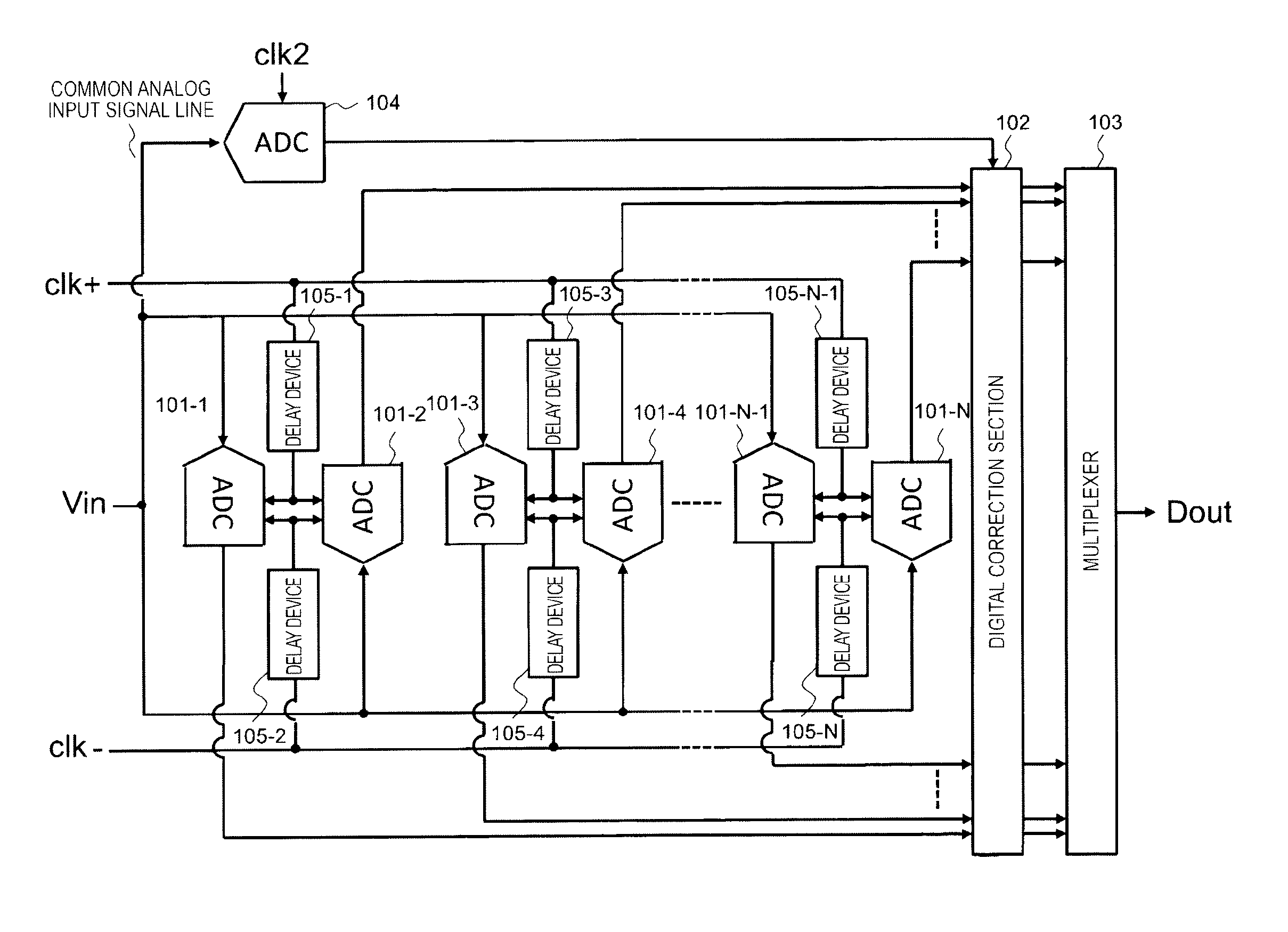
[0031]FIG. 1 illustrates an embodiment of an interleaved ADC according to a first embodiment.

[0032]In the embodiment, analog input terminals of N ADCs 101-k (k=integer from 1 to N and N is a multiple of 2) having differential input clock terminals are connected to a common analog input signal line. In addition, an input terminal of a reference ADC 104 is connected to the common analog input signal line.

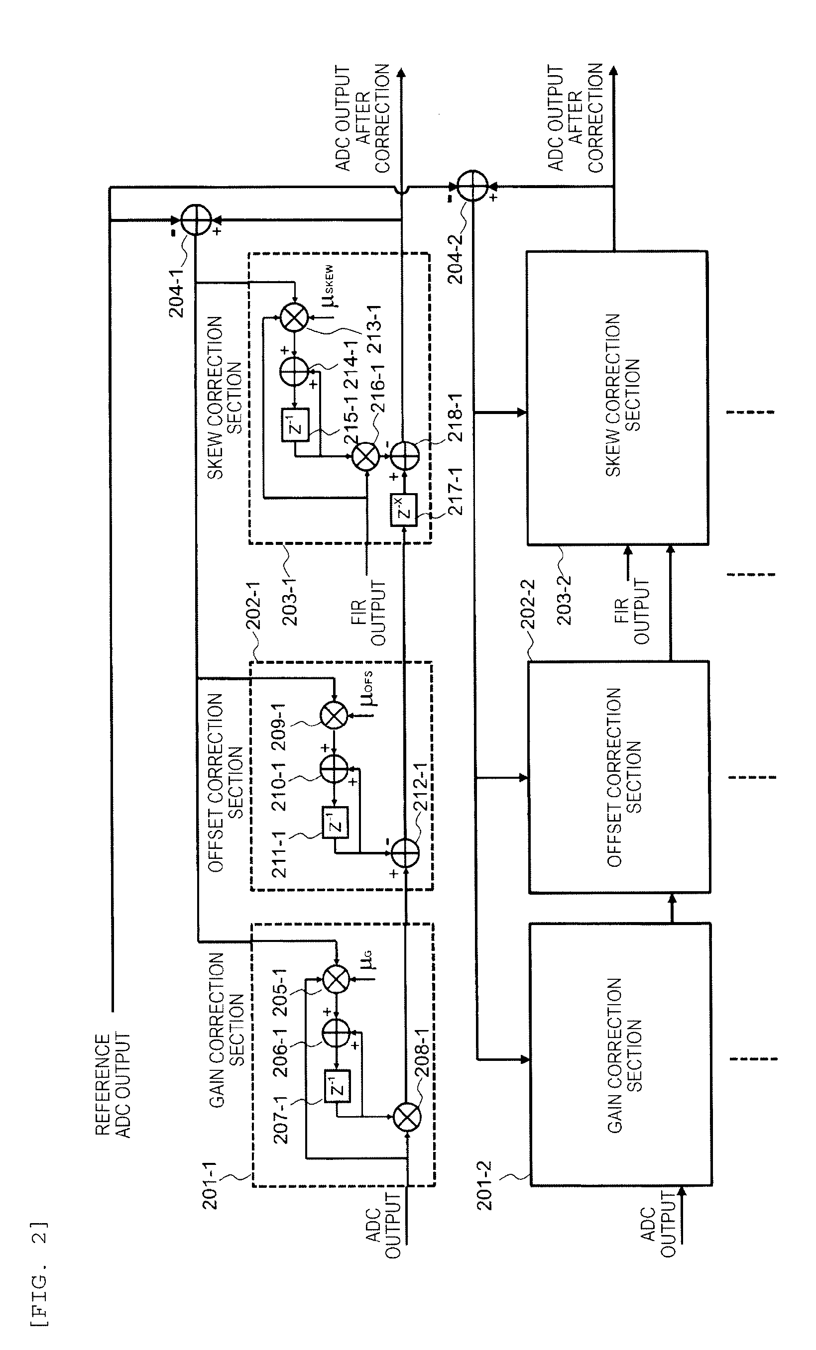
[0033]Here, the ADC 101-k and the reference ADC 104 include an input sampling circuit. A digital output of each ADC 101-k is connected to a digital correction section 102 and a mismatch between each of AD conversion paths such as DC offset, deviation of conversion gain, and a shift of sampling timing that occur in each AD conversion path is corrected from comparison an output of the ADC 104 with an output of each ADC 101-k. Hereinafter, in each ADC 101-k, ideal sampling timing, without shifting, refers to timing as sampling intervals are equal to each other between adjacent ADCs 101-k...

second embodiment

[0057]FIG. 4 illustrates an embodiment of an interleaved ADC according to a second embodiment.

[0058]The embodiment illustrates an example of solutions for further reduce the problem in which the kickback component of the ADC in the first embodiment disturbs the input signal.

[0059]In the embodiment, analog input terminals of N ADCs 101-k (k=integer of 1 to N and N is a multiple of 2) having differential input clock terminals are connected to an output terminal of a buffer section 401-k and an input terminal of the buffer section 401-k is connected to a common analog input signal line. In addition, an input terminal of a buffer section 400 is connected to the common input signal line and an input terminal of the reference ADC 104 is connected to an output terminal of the buffer section 400. Here, the ADC 101-k and the reference ADC 104 include an input sampling circuit. A digital output of each ADC 101-k is connected to the digital correction section 102 and similar to the first embod...

third embodiment

[0071]FIG. 5 illustrates an embodiment of an interleaved ADC according to a third embodiment.

[0072]The embodiment is provided to digitally correct characteristics of a buffer section to prevent degradation of the characteristics by providing the buffer section disclosed in the second embodiment.

[0073]The embodiment is configured of N ADCs 101-k (k=natural number of 1 to N), the buffer sections 401-k respectively connected to an analog input terminal of the ADC 101-k, the multiplexer 103 connected to an output terminal of the digital correction section 102 connected to each ADC 101-k, the buffer section 400 of which an input terminal is connected to a common input signal line, and the reference ADC 104 of which an input terminal is connected to an output terminal of the buffer section 400.

[0074]Here, the ADC 101-k and the reference ADC 104 include input sampling circuits. An analogue signal Vin is input into each buffer section 401-k and a sampling clock signal having a frequency fs ...


PUM


Abstract

It is a problem that each ADC sampling circuit connected in parallel in an interleaved ADC releases an electric charge depending on an input signal when sampling is performed and other ADCs connected in parallel sample the input signal disturbed thereby so that resolution of the interleaved ADC is decreased.
The problem is improved by inputting a common differential sampling clock signal to one set of two ADCs which is sampled at a π-phase shift of each ADC connected in parallel in a time interleaved ADC, providing an individual buffer in a prior stage of an input sampling circuit, isolating a common analog input signal line from an ADC input terminal, and digitally correcting characteristics degradation by insertion of the buffer.

Description

TECHNICAL FIELD[0001]The present invention relates to an interleaved A / D converter.BACKGROUND ART[0002]An analog / digital converter (hereinafter, referred to as ADC) is required for a computer that is operated by a digital signal to process physical information converted into an analog electrical signal by a sensor.[0003]High performance is always required for the ADC used in a measuring device according to requirement of performance improvement of a measuring apparatus such as an inspection apparatus that is used for manufacturing semiconductors in which miniaturization is processed and a medical diagnostic apparatus having a high speed and high resolution for more accurate diagnosis.[0004]However, a speed of single ADC that can perform sampling while maintaining an effective resolution in 10 bit or more may be limited to approximately 250 MHz from rate-limiting derived from frequency characteristics of a transistor configuring the ADC.[0005]Thus, a technique called time interleavin...

Claims


Application Information

Patent Timeline
Patent Type & Authority Applications(United States)
IPC IPC(8): H03M1/06H03M1/36H03M1/12
CPCH03M1/0626H03M1/36H03M1/1245H03M1/121H03M1/0624H03M1/1215
Inventor NAKAMURA, YOHEIOSHIMA, TAKASHI
Owner HITACHI LTD
Why Eureka
Try Eureka