Micro-pillar assisted semiconductor bonding

Active Publication Date: 2015-12-17
SKORPIOS TECH
View PDF7 Cites 2 Cited by
  • Summary
  • Abstract
  • Description
  • Claims
  • Application Information

AI Technical Summary

Benefits of technology

The patent text discusses a method for bonding a semiconductor material to another semiconductor material using micro pillars. These pillars help to break indium oxide and penetrate into the indium during the bonding process, improving the electrical contact and reducing the amount of heat transferred to the silicon surface. The technical effect of this method is improved bonding between different semiconductor materials, with reduced heat transfer and improved functionality.

Problems solved by technology

Bonding a planar silicon surface to a planar III-V material using indium has some challenges.
Yet indium oxide can form on indium before or during bonding, thus reducing functionality of the electrical contact.
If the silicon is planar, the silicon acts as a heat sink, making heating of the indium more difficult.

Method used


Image

  • Micro-pillar assisted semiconductor bonding
  • Micro-pillar assisted semiconductor bonding
  • Micro-pillar assisted semiconductor bonding

Examples


Embodiment Construction

[0018]The ensuing description provides preferred exemplary embodiment(s), and is not intended to limit the scope, applicability, or configuration of the disclosure. Rather, the ensuing description of the preferred exemplary embodiment(s) will provide those skilled in the art with an enabling description for implementing a preferred exemplary embodiment. It is understood that various changes may be made in the function and arrangement of elements without departing from the spirit and scope as set forth in the appended claims.

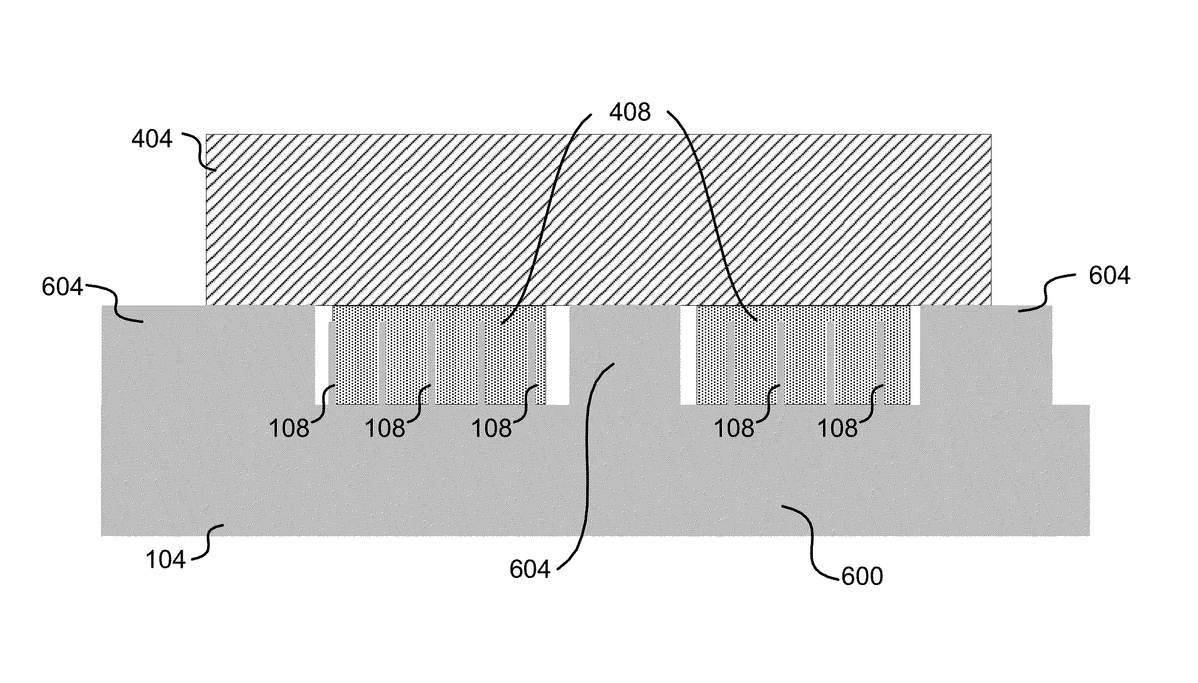
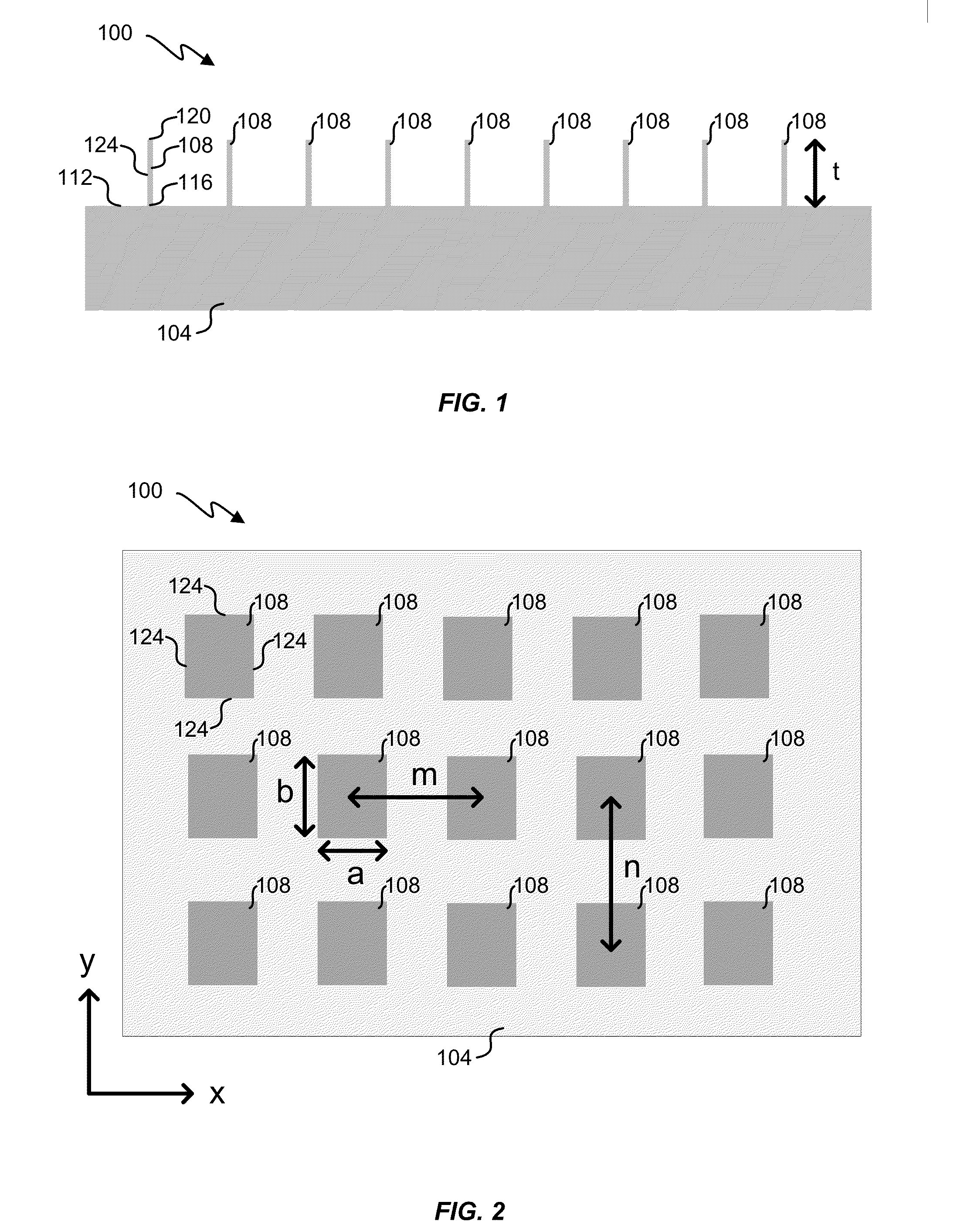
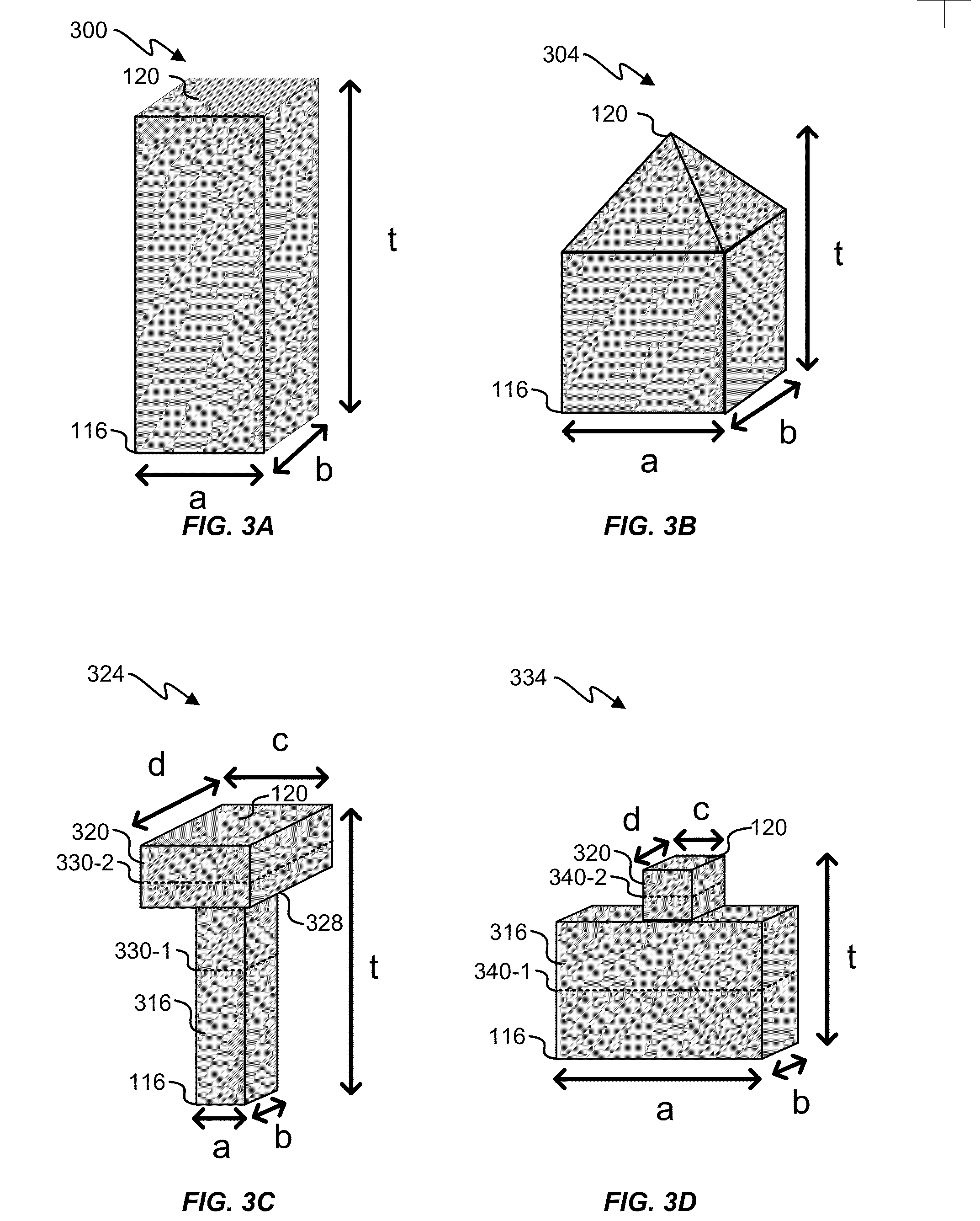
[0019]Referring to FIG. 1, a side view of an embodiment of a first semiconductor 100 comprising a substrate 104 and a plurality of pillars 108 is shown. The pillars 108 extend from the substrate 104 in a direction normal to a top surface 112 of the substrate 104. In some embodiments, the substrate 104 and / or the pillars 108 are made of silicon (e.g., crystalline silicon). The pillars 108 can be formed using lithography (e.g., etched from a same wafer, such as a s...


PUM


Abstract

Micro pillars are formed in silicon. The micro pillars are used in boding the silicon to hetero-material such as III-V material, ceramics, or metals. In bonding the silicon to the hetero-material, indium is used as a bonding material and attached to the hetero-material. The bonding material is heated and the silicon and the hetero-material are pressed together. As the silicon and the hetero-material are pressed together, the micro pillars puncture the bonding material. In some embodiments, pedestals are used in the silicon as hard stops to align the hetero-material with the silicon.

Description

CROSS-REFERENCES TO RELATED APPLICATIONS[0001]This application claims priority to U.S. Provisional Application No. 62 / 012,814, filed on Jun. 16, 2014, the disclosure of which is incorporated by reference in its entirety for all purposes.BACKGROUND[0002]Silicon integrated circuits have dominated the development of electronics and many technologies based upon silicon processing have been developed over the years. Their continued refinement led to nano-scale feature sizes that can be important for making metal oxide semiconductor CMOS circuits. On the other hand, silicon is not a direct-bandgap material. Although direct-bandgap materials, including III-V compound semiconductor materials, have been developed, there is a need in the art for improved methods and systems related to photonic integrated circuits utilizing silicon substrates.[0003]This application relates to bonding a first semiconductor to a second semiconductor. More specifically, and without limitation, to bonding a III-V ...

Claims


Application Information

Patent Timeline
IPC IPC(8): H01L23/00
CPCH01L24/80H01L24/09H01L2224/0912H01L2224/80139H01L2224/0951H01L2224/80097H01L2224/0905H01L24/83H01L2224/3003H01L2224/3012H01L2224/83012H01L2224/1161H01L2224/14131H01L2224/29017H01L2224/32147H01L2224/83139H01L2224/83902H01L24/03H01L24/11H01L24/13H01L24/29H01L24/30H01L24/73H01L24/81H01L24/92H01L25/0657H01L2224/0361H01L2224/04026H01L2224/05557H01L2224/05638H01L2224/13013H01L2224/13017H01L2224/13018H01L2224/13019H01L2224/136H01L2224/29082H01L2224/29109H01L2224/32145H01L2224/73204H01L2224/81191H01L2224/8301H01L2224/83048H01L2224/8314H01L2224/83191H01L2224/83385H01L2224/83815H01L2224/9211H01L2224/81903H01L2224/13138H01L2225/06555H01L25/50H01L2225/06513H01L24/05H01L2924/01014H01L2924/00014H01L2924/00012H01L2224/81H01L2224/83G02B6/4232G02B6/423G02B6/3636G02B6/4245H01L21/2007H01L23/3178H01L21/187
Inventor LAMBERT, DAMIEN
Owner SKORPIOS TECH
Why Eureka
Try Eureka