Pixel Structure for OLED Display and Metal Mask Thereof

a metal mask and oled display technology, applied in the field of display technique, can solve the problems of low yield during production, easy damage or deformation of metal masks, low repeatability rate, etc., and achieve the effect of improving the resolution of the oled display and enhancing the strength of the metal mask

Active Publication Date: 2015-12-17
KUNSHAN VISIONOX DISPLAY TECH +1
View PDF4 Cites 41 Cited by
  • Summary
  • Abstract
  • Description
  • Claims
  • Application Information

AI Technical Summary

Benefits of technology

[0041]The pixel structure and its corresponding metal mask and OLED display of the present disclosure has the following advantages.
[0042]The distance between the corresponding openings of the sub pixels are widened when making the corresponding metal mask to enhance the strength of the metal mask that a pixel unit of a smaller size can be produced under the consideration of process condition, so as to improve the resolution of the OLED display.

Problems solved by technology

This creates a problem that the metal strip is likely to be out of shape under the influence of magnetic field lines of the magnetic board during the use of the metal mask, resulting in color mixing caused by the spread of different color materials in among pixels, and resulting in low yield during production.
Moreover, this kind of metal mask is easy to be damaged or deformed in the process of using, cleaning and storing, with a low repetitive use rate, and the screen produced by this mode has a high cost due to the high cost of the metal mask.
Because both the above Slit Mode and Slot Mode have defects, the opening mode of the blue metal mask (B mask) of the arrangement of the pixel array as shown in FIG. 4 seriously affects the opening rate of the sub pixel and the resolution further upgrade.

Method used


Image

  • Pixel Structure for OLED Display and Metal Mask Thereof
  • Pixel Structure for OLED Display and Metal Mask Thereof
  • Pixel Structure for OLED Display and Metal Mask Thereof

Examples


Embodiment Construction

[0058]In the following description of embodiments, reference is made to the accompanying drawings which form a part hereof, and in which it is shown by way of illustration specific embodiments of the present disclosure that can be practiced. It is to be understood that other embodiments can be used and structural changes can be made without departing from the scope of the disclosed embodiments.

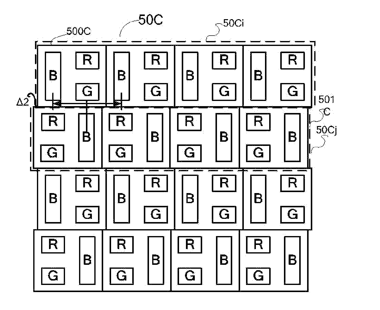
[0059]FIGS. 8 (a)-8(c) illustrate a pixel structure of the OLED display according to one embodiment of the present disclosure.

[0060]Wherein, a pixel structure 50A is located on a substrate (not shown). The pixel structure 50A includes multi-row pixel unit groups (denoted with the dotted box), a plurality of pixel unit groups in odd rows 50Ai includes pixel units 500A arranged repeatedly, and a plurality of pixel unit groups in even rows 50Aj includes pixel units 501A arranged repeatedly.

[0061]Wherein, each pixel unit 500A or 501A can be a square, each pixel unit 500A or 501A includes red (R), ...


PUM


Abstract

A pixel structure for OLED display is disclosed. The pixel structure includes multi-row pixel unit groups, each pixel unit group includes a plurality of pixel units arranged repeatedly in sequence, and each pixel unit includes a first sub pixel, a second sub pixel and a third sub pixel, wherein the same sub pixels of the pixel units in adjacent two rows are arranged in dislocation in a horizontal direction. The pixel structure can widen the distance between the corresponding openings of the sub pixels when making the corresponding metal mask to enhance the strength of the metal mask that a pixel unit of a smaller size can be produced under the consideration of process condition, so as to improve the resolution of the OLED display.

Description

FIELD OF THE INVENTION[0001]The present disclosure relates generally to the field of display technique, and specifically to a high resolution pixel structure and a fine metal mask corresponding to the pixel structure.BACKGROUND OF THE INVENTION[0002]Compared with traditional LCD display mode, it is not necessary for OLED display technique to use backlights. The OLED display technique has the property of self-illumination, a very thin organic material film and a glass substrate are used, and the organic material can glow when an electric current passes through it. Therefore an OLED display can provide significant power savings, can be lighter and thinner, and can tolerate a wider range of temperature variation than LCDs, with a wider viewing angle. The light-emitting layer of the OLED screen is composed by organic light-emitting components formed on corresponding pixel locations on an array substrate by using evaporation film technology to organic materials through a fine metal mask....

Claims


Application Information

Patent Timeline
Patent Type & Authority Applications(United States)
IPC IPC(8): H01L27/32
CPCH01L27/3216H01L27/3218H10K59/352H10K59/353H10K59/35
Inventor PENG, CHAOCHIQIU, YONGZHANG, SHENFU
Owner KUNSHAN VISIONOX DISPLAY TECH
Why Eureka
Try Eureka