
Semiconductor device and method for manufacturing same

Inactive Publication Date: 2015-12-24
LONGITUDE SEMICON S A R L
View PDF1 Cites 16 Cited by
  • Summary
  • Abstract
  • Description
  • Claims
  • Application Information

AI Technical Summary

Benefits of technology

The present invention provides a semiconductor device and a method for manufacturing it, which involves the use of thin barrier metal films that maintain adhesion with the metal electrode and can be controlled / managed in thickness. This is achieved through a method where a trench is formed in a semiconductor substrate, a gate insulating film is formed inside the trench, a first barrier metal is formed on the gate insulating film under a first film formation condition, a second barrier metal is formed on the first barrier metal under a second film formation condition different than the first film formation condition, a metallic material is formed on the second barrier metal in such a way as to fill the trench, and the longitudinal parts of the trench are filled with a cap insulating film. This method allows for the formation of thin barrier metal films, maintaining adhesion with the metal electrode and allowing for control and management of the thickness of the thin film.

Problems solved by technology

As memory cells comprising a cell transistor provided in this kind of semiconductor device become miniaturized, this leads to problems such as a deterioration in transistor characteristics caused by the short channel effect, and an increase in contact resistance caused by a reduction in the diameter of contact holes.

Method used


Image

  • Semiconductor device and method for manufacturing same
  • Semiconductor device and method for manufacturing same
  • Semiconductor device and method for manufacturing same

Examples


exemplary embodiment 1

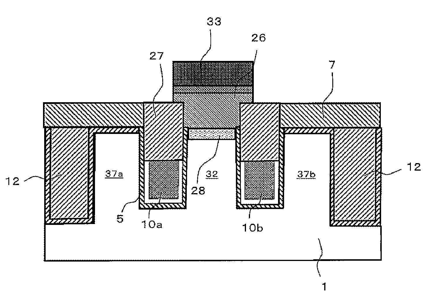
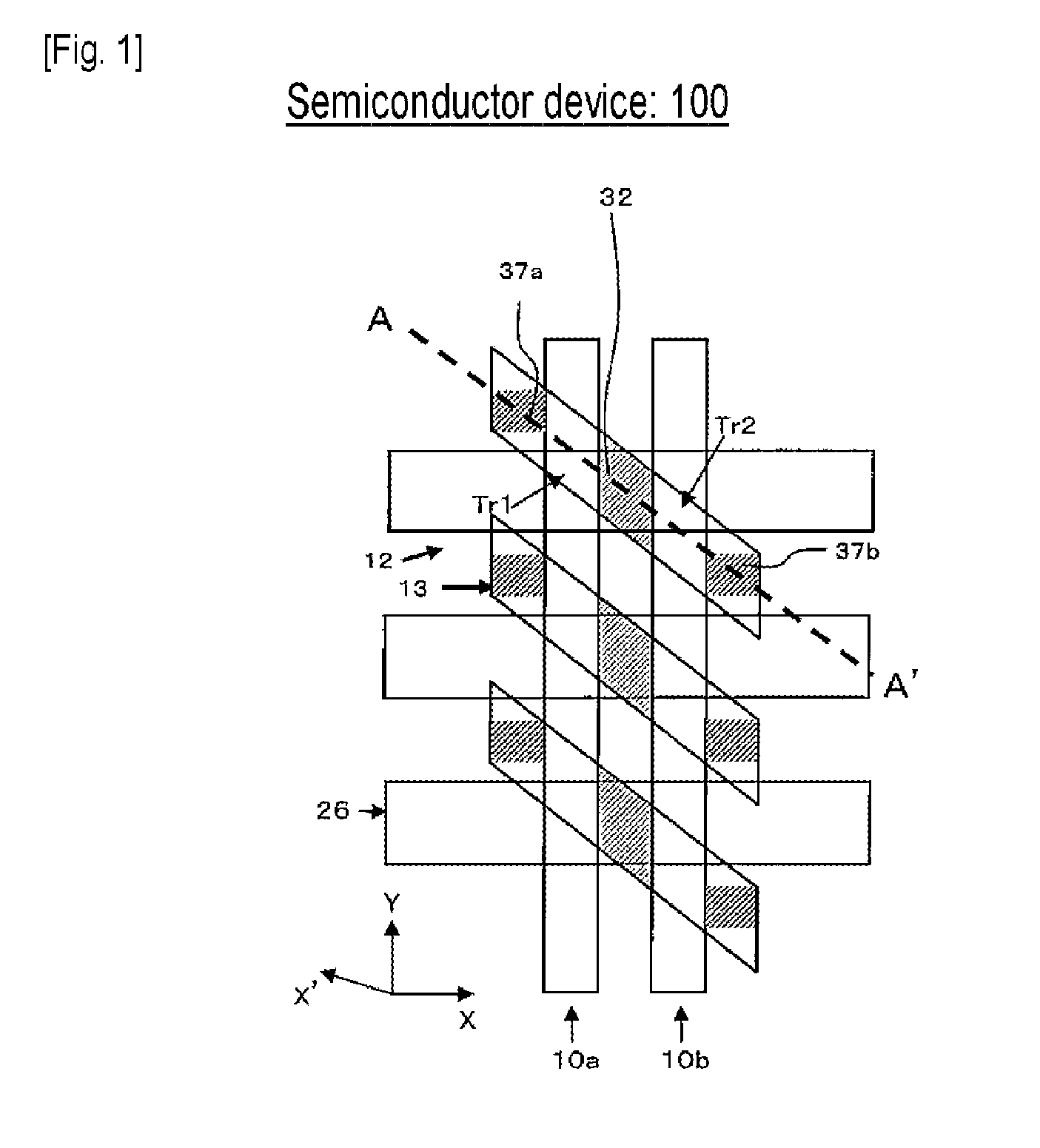
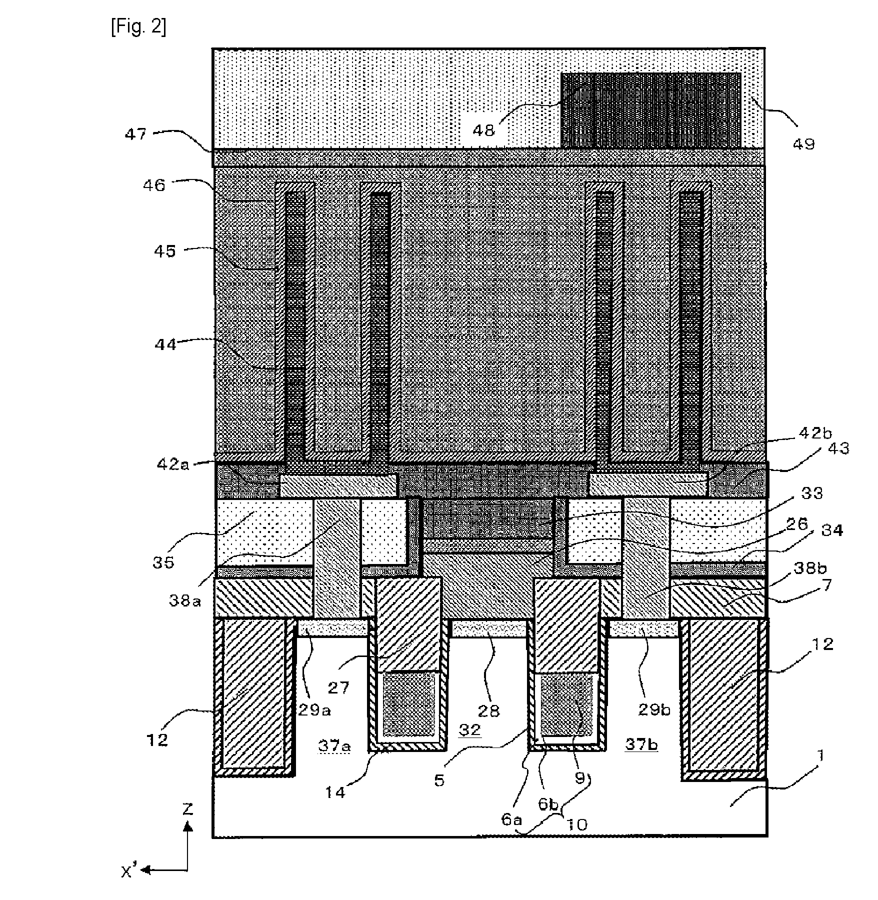
[0048]A first exemplary embodiment of the present invention will be described in detail below with reference to the figures.

[0049]In the following figures, the scale and number etc. of each structure differs from the actual structures in order to facilitate an understanding of the constituent elements. Furthermore, the arrangement of each constituent element will be described by setting an XYZ coordinate system. In this coordinate system, the Z-direction is a direction perpendicular to the surface of a silicon substrate constituting a semiconductor substrate, the X-direction is a direction orthogonal to the Z-direction in a plane which is level with the surface of the silicon substrate, and the Y-direction is a direction orthogonal to the X-direction in a plane which is level with the surface of the silicon substrate. Furthermore, the X′-direction is a direction which is obliquely inclined with respect to the X-direction.

[0050]FIG. 1 to FIG. 10 show the structure of a semiconductor ...


PUM


Abstract

One semiconductor device includes an active region on a semiconductor substrate, a trench having a lower section and an upper section within the active region, a gate insulating film that covers the inner wall surface of the trench, a first barrier metal that covers the lower section of the trench interposed by the gate insulating film, a second barrier metal that covers the first barrier metal, and a metal electrode that covers the second barrier metal and fills up the lower section of the trench. The second barrier metal is thinner than the first barrier metal.

Description

TECHNICAL FIELD[0001]The present invention relates to a semiconductor device and to a method for manufacturing same, and in particular the present invention relates to effective technology for application to a semiconductor device comprising a DRAM (dynamic random access memory) employing an embedded word line structure.BACKGROUND[0002]A DRAM, which is a type of semiconductor memory device, is installed in a large number of varying electronic devices used by people in daily life. Furthermore, there is also a strong demand for higher performance from installed DRAMs, in terms of reduced power, higher speed and higher capacity, which has come about with the recent need for lower power consumption and higher performance in devices.[0003]One of the most effective means for achieving high performance in a DRAM is to miniaturize a memory cell. The length of word lines and bit lines connected to the memory cell decreases as a result of miniaturizing the memory cell. The parasitic capacitan...

Claims


Application Information

Patent Timeline
IPC IPC(8): H01L27/108H01L29/423H01L29/49H01L21/28
CPCH01L27/10823H01L21/28088H01L29/4966H01L27/10876H01L29/4236H01L29/66621H10B12/34H10B12/315H10B12/053H10B12/488H10B12/485H10B12/482
Inventor NOBUTO, HIDEKAZU
Owner LONGITUDE SEMICON S A R L
Learn More