Photomask and method for manufacturing photomask

a technology of photomask and manufacturing method, which is applied in the field of photomask and a manufacturing method of photomask, can solve the problems of reducing the life of the photomask, affecting the appearance of the face, so as to reduce the cost, reduce the operating temperature, and speed up the manufacturing process

a technology of photomask and manufacturing method, which is applied in the field of photomask and a manufacturing method of photomask, can solve the problems of reducing the life of the photomask, affecting the appearance of the face, so as to reduce the cost, reduce the operating temperature, and speed up the manufacturing process

US20150378252A1Active Publication Date: 2015-12-31NAT CHENG KUNG UNIV

Image

  • Photomask and method for manufacturing photomask
  • Photomask and method for manufacturing photomask
  • Photomask and method for manufacturing photomask

Examples


Embodiment Construction

[0030]The present invention will be apparent from the following detailed description, which proceeds with reference to the accompanying drawings, wherein the same references relate to the same elements. In the following embodiments and drawings, the elements and the steps which do not directly relate to the invention are omitted. Moreover, the size ratio of various elements is only for easily understanding but not for limiting the actual proportion.

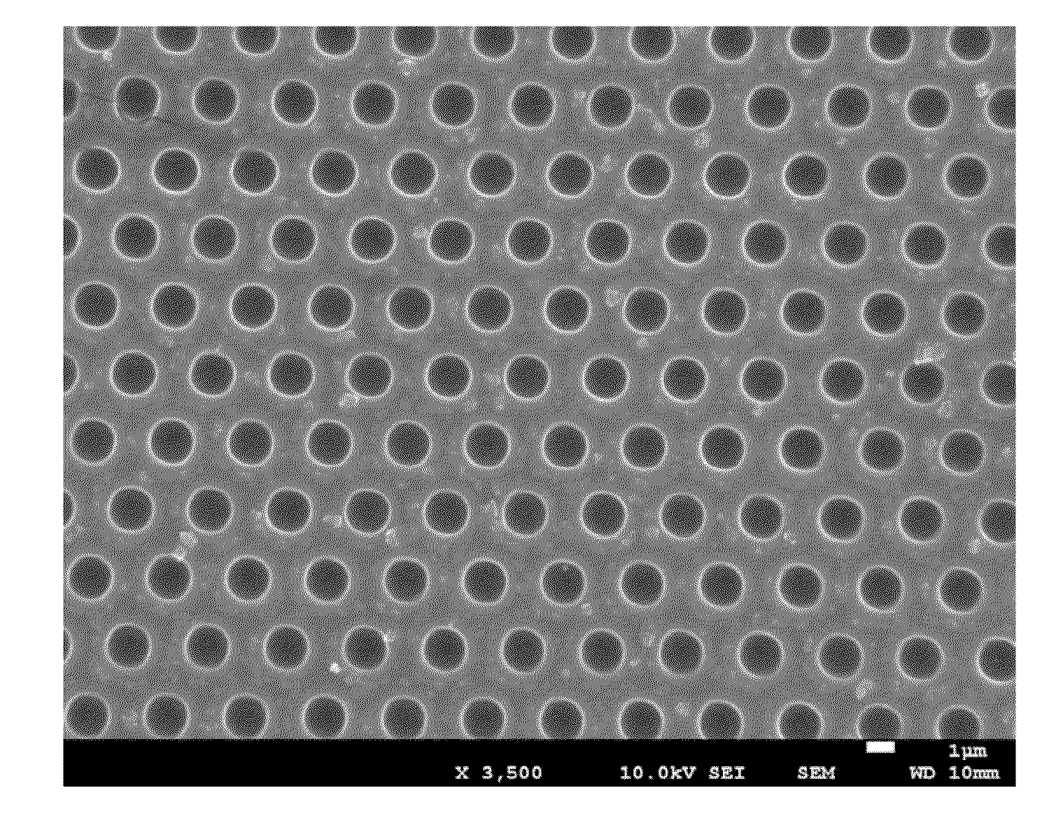
[0031]It is noted that the photomask and the method for manufacturing a photomask according to the invention may be applied to the photolithography processes of semiconductor or optoelectronic display, or it may be applied to the photolithography process during manufacturing a patterned sapphire substrate of a light-emitting diode, but they are not limited to the above applications. Moreover, the photomask according to the invention may be a contact three-dimensional photomask.

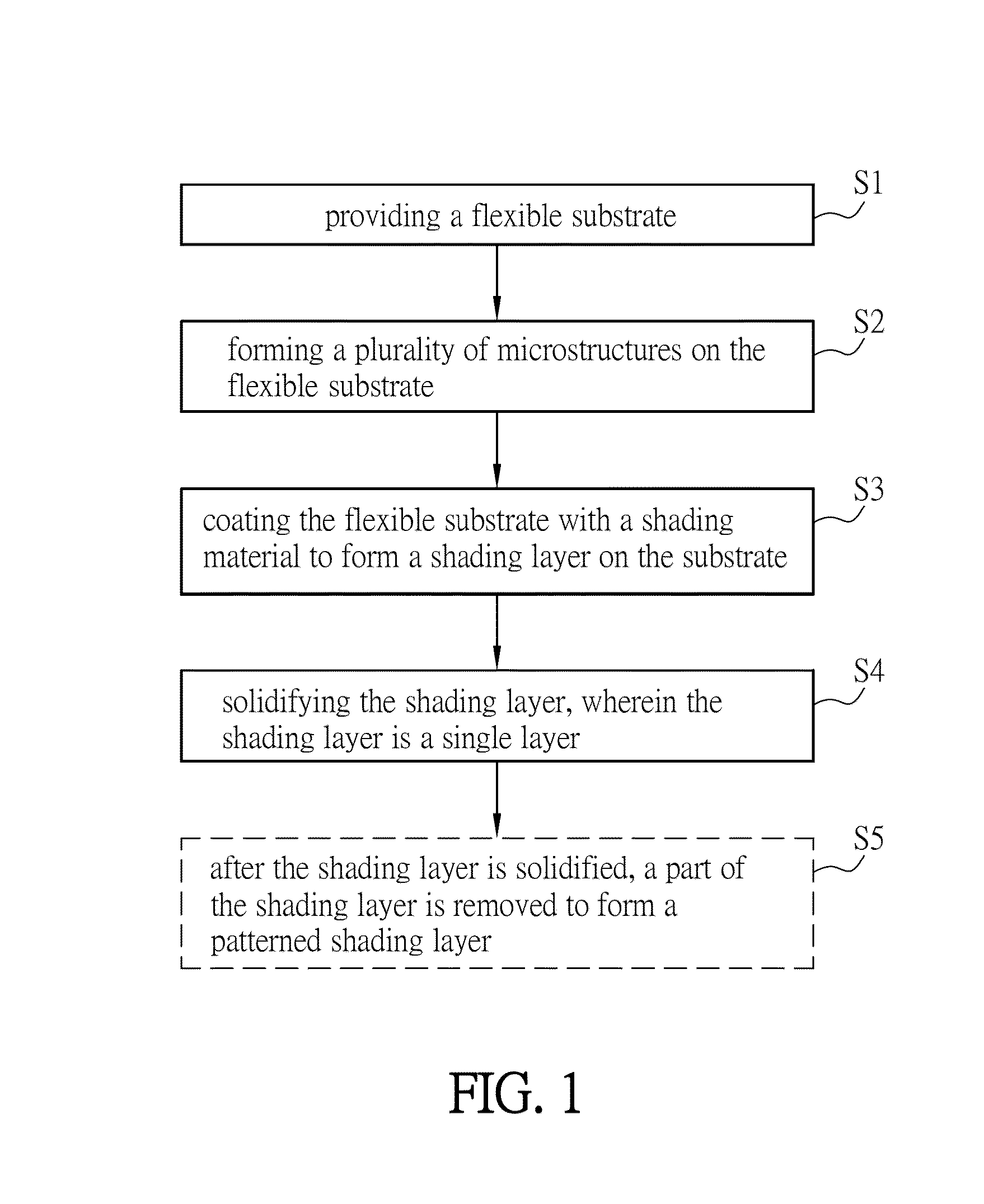
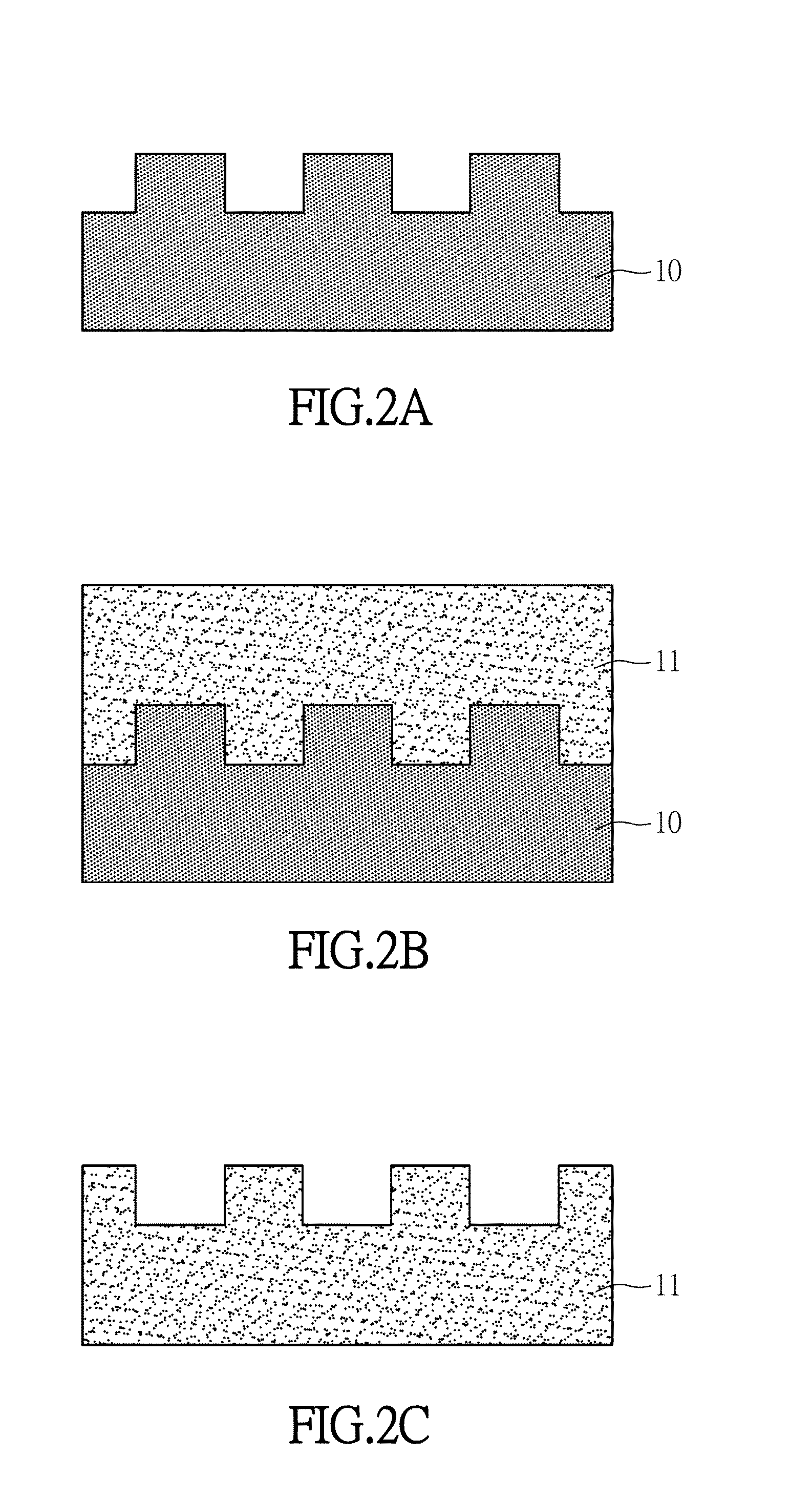
[0032]Referring to FIGS. 1 to 2F, FIG. 1 is a flow chart of ma...


PUM

PropertyMeasurementUnit
temperatureaaaaaaaaaa
thicknessaaaaaaaaaa
temperatureaaaaaaaaaa

Abstract

A method for manufacturing a photomask is provided. The method includes providing a flexible substrate, forming a plurality of microstructures on the flexible substrate, coating the flexible substrate with a shading material to form a shading layer on the substrate, and solidifying the shading layer which is a single layer.

Description

CROSS REFERENCE TO RELATED APPLICATIONS[0001]This Non-provisional application claims priority under 35 U.S.C. ยง119(a) on Patent Application No(s). 103122469 filed in Taiwan, Republic of China on Jun. 30, 2014, the entire contents of which are hereby incorporated by reference.BACKGROUND OF THE INVENTION[0002]1. Field of Invention[0003]The invention relates to a photomask and a method for manufacturing a photomask.[0004]2. Related Art[0005]In conventional photolithography, utilizing the photomask to proceed with the ultraviolet (UV) exposure on the photoresist layer is mainly classified into contact photolithography and reticle lithography.[0006]In contact photolithography, the size ratio of the feature pattern on the surface of the photomask and the pattern actually replicated on the substrate is 1:1, and the photomask is directly very close to or nearly contacts the surface of the photoresist layer during the exposure. In reticle lithography, the size of the feature pattern on the s...

Claims


Application Information

Patent Timeline
31 Dec 2015
Publication
US20150378252A1
IPC
G03F1/38
CPC
G03F1/38
Inventors
LEE, YUNG-CHUN; WU, CHUN-YING