Opto-electronic micro-module and method for forming the same
a micro-module and optoelectronic technology, applied in the field of optoelectronic micro-modules and methods for forming the same, can solve the problems of low efficiency of optical coupling, large number of parts, complex assembly alignment, etc., and achieve low fabrication cost, wide range of operation temperature, and reduced volume
- Summary
- Abstract
- Description
- Claims
- Application Information
AI Technical Summary
Benefits of technology
Problems solved by technology
Method used
Image

Examples
first embodiment
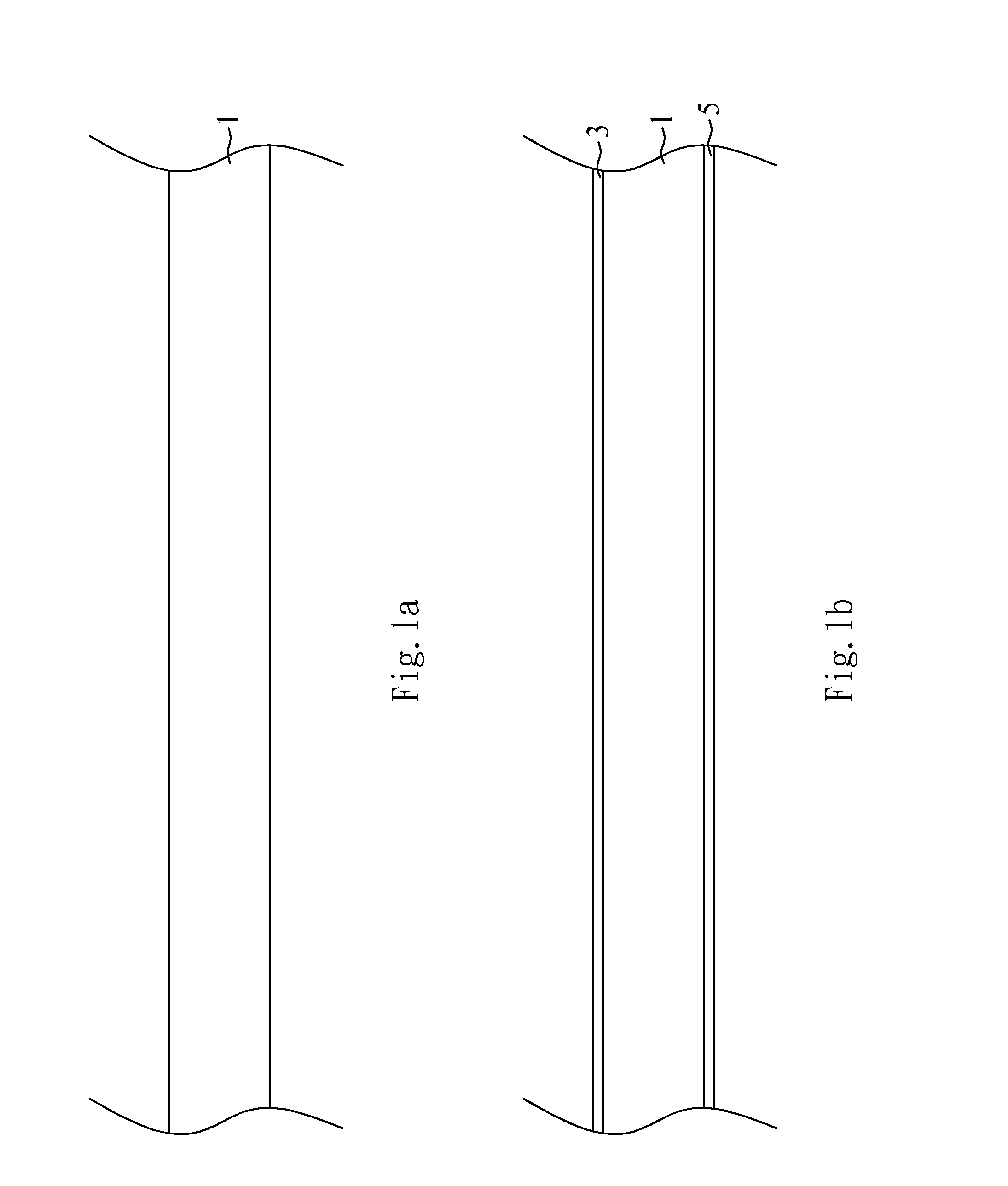
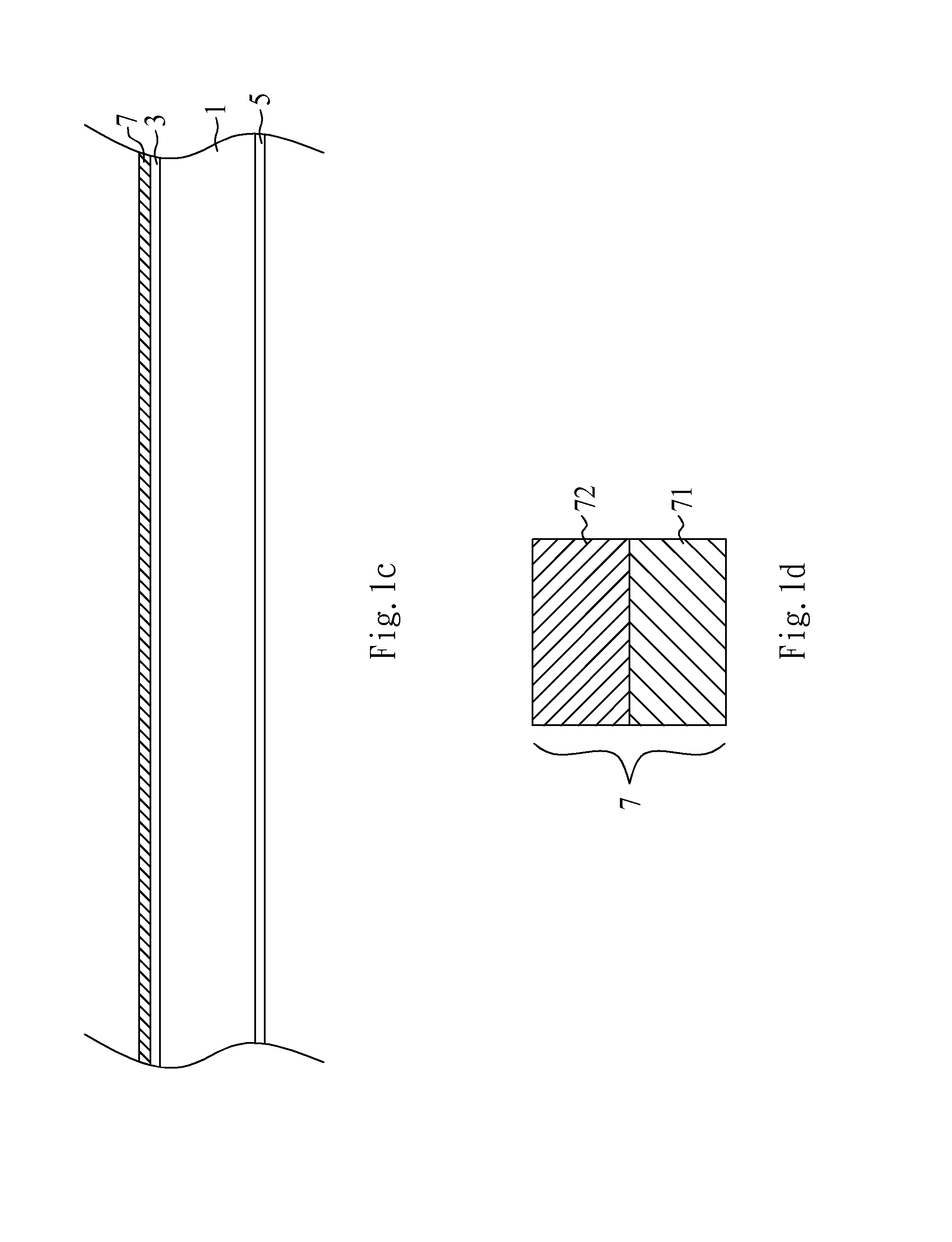
[0025]FIGS. 1a-1s are cross-sectional views illustrating a process for forming a substrate in accordance with a first embodiment of the present invention. FIGS. 2a-2e are cross-sectional views illustrating a process for forming an optical substrate, such as optical splitter, in accordance with the first embodiment of the present invention. FIG. 2f is a perspective view of the optical substrate, such as optical splitter, shown in FIG. 2e in accordance with the first embodiment of the present invention. FIGS. 3a-3h are cross-sectional views illustrating a process for assembling the optical substrate, such as optical splitter, and the substrate in accordance with the first embodiment of the present invention. FIGS. 4a-4d are cross-sectional views illustrating a process for assembling an opto-electronic micro-module in accordance with the first embodiment of the present invention. FIG. 5 is a cross-sectional view illustrating optical-signal transmission of an opto-electronic micro-modul...
second embodiment
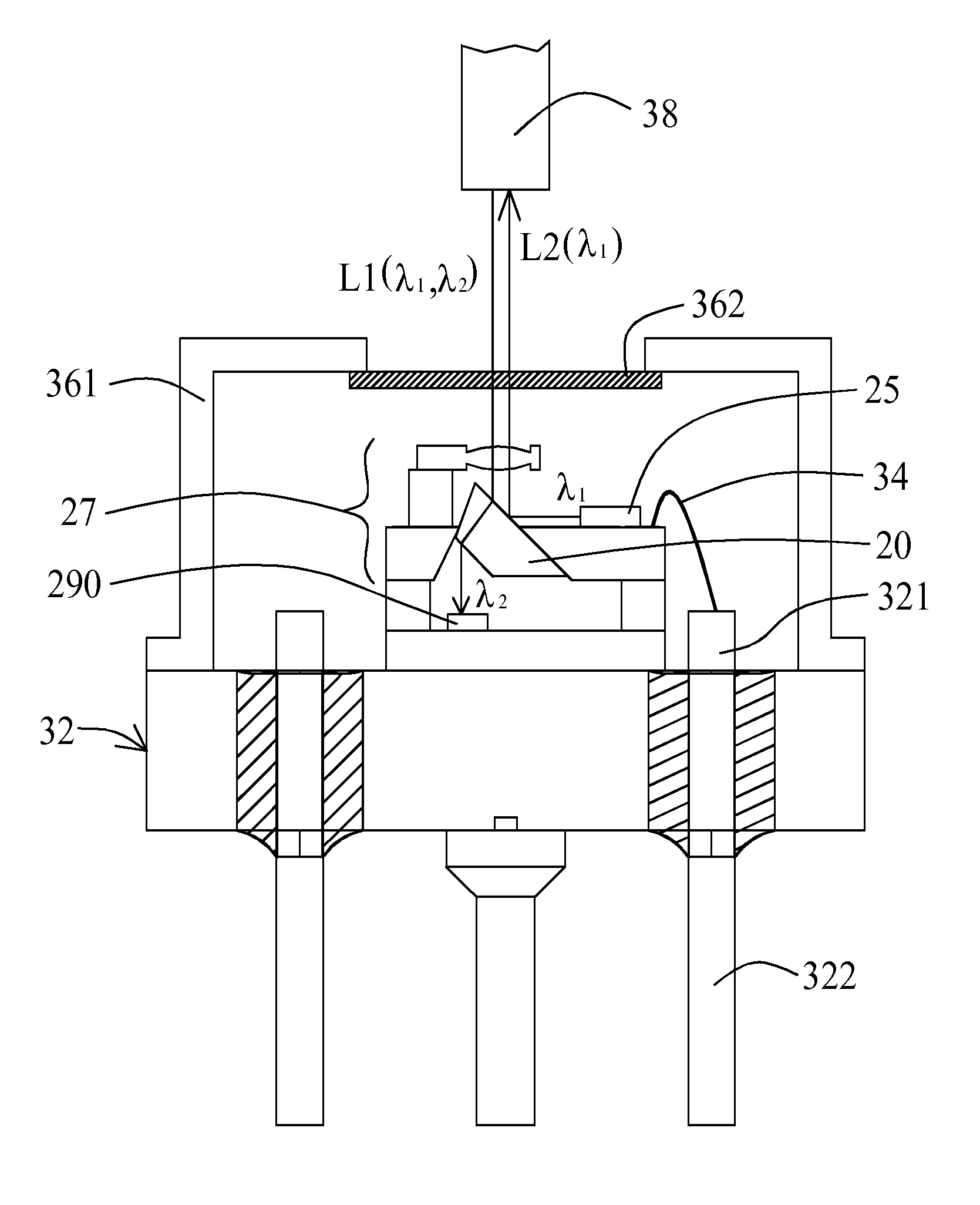
[0058]The second embodiment as illustrated in FIG. 6 is similar with the first embodiment. The difference between the first and second embodiments is that the positions of the optical-signal receiver 290 and the light emitting device 25 are replaced with each other and the optically reflective layers 19 of the optical substrates 20 in the first and second embodiments may have different rates of reflection and penetration. In this embodiment, multiple downlink optical signals L1 transmitted from the optical fiber 38 may include the first and second optical signals as illustrated in the first embodiment. The downlink optical signals L1 may pass through the transparent sheet 362 to be focused on the optically reflective layer 19 of the optical substrate 20, such as optical splitter, by the micro-lens 232. The optically reflective layer 19 may have the second optical signal to be reflected to the optical-signal receiver 290 and have the first optical signal to be refracted through the s...
third embodiment
[0059]The third embodiment as illustrated in FIG. 7 is similar with the second embodiment. The difference between the second and third embodiments is that the optical-signal receiver 290 in the second embodiment is replaced with another light emitting device 42 as seen in the third embodiment and the optically reflective layers 19 of the optical substrates 20 in the second and third embodiments may have different rates of reflection and penetration. In this embodiment, an optical-signal receiver 40 is arranged over the opto-electronic micro-module, wherein the optical-signal receiver 40 may be an infrared sensor, ultraviolet sensor, color sensor, optical-fiber sensor, charge-coupled image sensor or complementary metal-oxide-semiconductor sensor. In this embodiment, upon receiving uplink electronic signals, the light emitting device 42 may convert the uplink electronic signals into the optical signals 1, including the first optical signal having the wavelength λ1, such as 1310 nm, an...
PUM
 Abstract
Description
Claims
Application Information
 - R&D
- Intellectual Property
- Life Sciences
- Materials
- Tech Scout
- Unparalleled Data Quality
- Higher Quality Content
- 60% Fewer Hallucinations
Browse by: Latest US Patents, China's latest patents, Technical Efficacy Thesaurus, Application Domain, Technology Topic, Popular Technical Reports.
© 2025 PatSnap. All rights reserved.Legal|Privacy policy|Modern Slavery Act Transparency Statement|Sitemap|About US| Contact US: help@patsnap.com