Composition, cured article, laminate, method for manufacturing underlying film, method for forming pattern, pattern and method for manufacturing a resist for semiconductor process

a technology of semiconductor process and cured article, which is applied in the direction of instruments, photomechanical devices, coatings, etc., can solve the problems of adhesion to molds, emerging adhesiveness between substrate and curable composition, etc., and achieves good in-plane uniform thickness, good adhesiveness, and small defect density

Inactive Publication Date: 2016-01-14
FUJIFILM CORP
View PDF3 Cites 22 Cited by
  • Summary
  • Abstract
  • Description
  • Claims
  • Application Information

AI Technical Summary

Benefits of technology

[0019]By the invention, it now became possible to provide a composition capable of producing an underlying film which demonstrates a good adhes...

Problems solved by technology

With progress of activities in the imprinting, there has been emerging a problem of adhesiveness between the substrate and the curable compositio...

Method used


Image

  • Composition, cured article, laminate, method for manufacturing underlying film, method for forming pattern, pattern and method for manufacturing a resist for semiconductor process
  • Composition, cured article, laminate, method for manufacturing underlying film, method for forming pattern, pattern and method for manufacturing a resist for semiconductor process
  • Composition, cured article, laminate, method for manufacturing underlying film, method for forming pattern, pattern and method for manufacturing a resist for semiconductor process

Examples


examples

[0166]The characteristics of the invention are described more concretely with reference to Production Examples and Examples given below. In the following Examples, the material used, its amount and the ratio, the details of the treatment and the treatment process may be suitably modified or changed not overstepping the scope of the invention. Accordingly, the invention should not be limitatively interpreted by the Examples mentioned below.

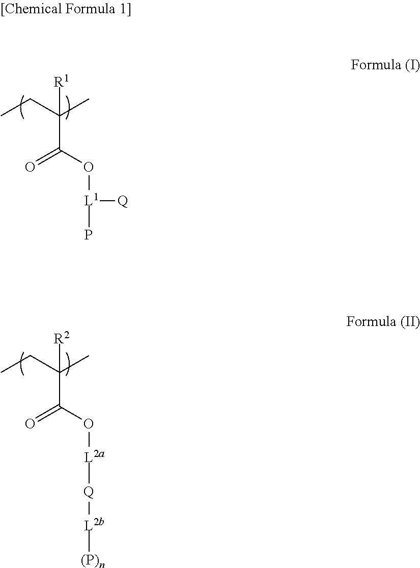
[0167]Each of the polymerizable compounds listed below was diluted by the first solvent and the second solvent summarized in Table below, further added with additives, so as to control the solid content of the polymerizable compound to 0.1% by mass. The mixture was filtered through a 0.1 pm PTFE filter to obtain a composition.

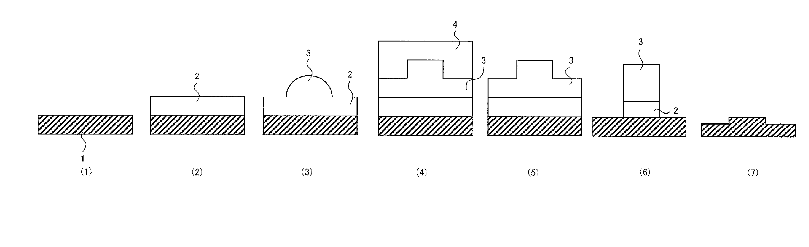
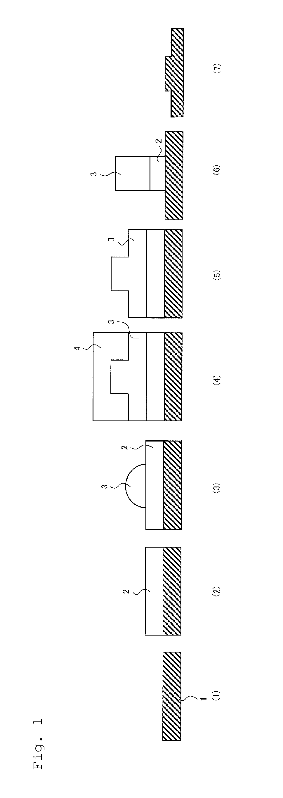
[0168]The composition was spin-coated over an SOG (Spin On Glass) film (surface energy=55 mJ / m2) formed on an 8-inch silicon wafer, and heated at the temperature summarized in Table below, on a hot plate for one minute. The co...


PUM

PropertyMeasurementUnit
Temperatureaaaaaaaaaa
Percent by massaaaaaaaaaa

Abstract

Provided is a composition capable of producing an underlying film which demonstrates a good adhesiveness between a substrate and a layer to be imprinted, showing a good in-plane uniformity of the thickness, and a small defect density. The composition includes a polymerizable compound, a first solvent, and a second solvent, the first solvent having a boiling point at 1 atm of 160° C. or higher, the second solvent having a boiling point at 1 atm of lower than 160° C., and the content of the polymerizable compound in the composition being less than 1% by mass.

Description

CROSS-REFERENCE TO RELATED APPLICATIONS[0001]This application is a Continuation of PCT International Application No. PCT / JP2014 / 058326 filed on Mar. 25, 2014, which claims priority under 35 U.S.C §119 (a) to Japanese Patent Application No. 2013-065612 filed on Mar. 27, 2013. Each of the above application(s) is hereby expressly incorporated by reference, in its entirety, into the present application.TECHNICAL FIELD[0002]This invention relates to a composition, a cured article obtained by curing the composition, and a laminate. This invention also relates to a method for manufacturing an underlying film, a method for forming a pattern, and a pattern formed by the method for forming a pattern, all using the composition described above. This invention further relates to a method for manufacturing a resist for semiconductor process using the method for forming a pattern.DESCRIPTION OF THE RELATED ART[0003]Nanoimprint technology is a development advanced from embossing technology well kno...

Claims


Application Information

Patent Timeline
IPC IPC(8): C09D133/14C09D133/08H01L21/02
CPCC09D133/14H01L21/02345C09D133/08C08F290/06C08F299/02C09D4/00C08F222/1067G03F7/0002G03F7/11
Inventor ENOMOTO, YUICHIROKITAGAWA, HIROTAKAOOMATSU, TADASHIGOTO, YUICHIRO
Owner FUJIFILM CORP
Why Eureka
Try Eureka