Frequency multiplier based on a low dimensional semiconductor structure

a semiconductor structure, low-dimensional technology, applied in the direction of oscillator, semiconductor device, electrical apparatus, etc., can solve problems such as distortion of input signal waveform

Inactive Publication Date: 2016-02-04
SOUTH CHINA NORMAL UNIVERSITY
View PDF5 Cites 5 Cited by
  • Summary
  • Abstract
  • Description
  • Claims
  • Application Information

AI Technical Summary

Benefits of technology

[0023]FIG. 3 is an output characteristic curve graph under the effect of two high-frequency signa...

Problems solved by technology

Non-linear elements will result in d...

Method used


Image

  • Frequency multiplier based on a low dimensional semiconductor structure
  • Frequency multiplier based on a low dimensional semiconductor structure
  • Frequency multiplier based on a low dimensional semiconductor structure

Examples


embodiment 1

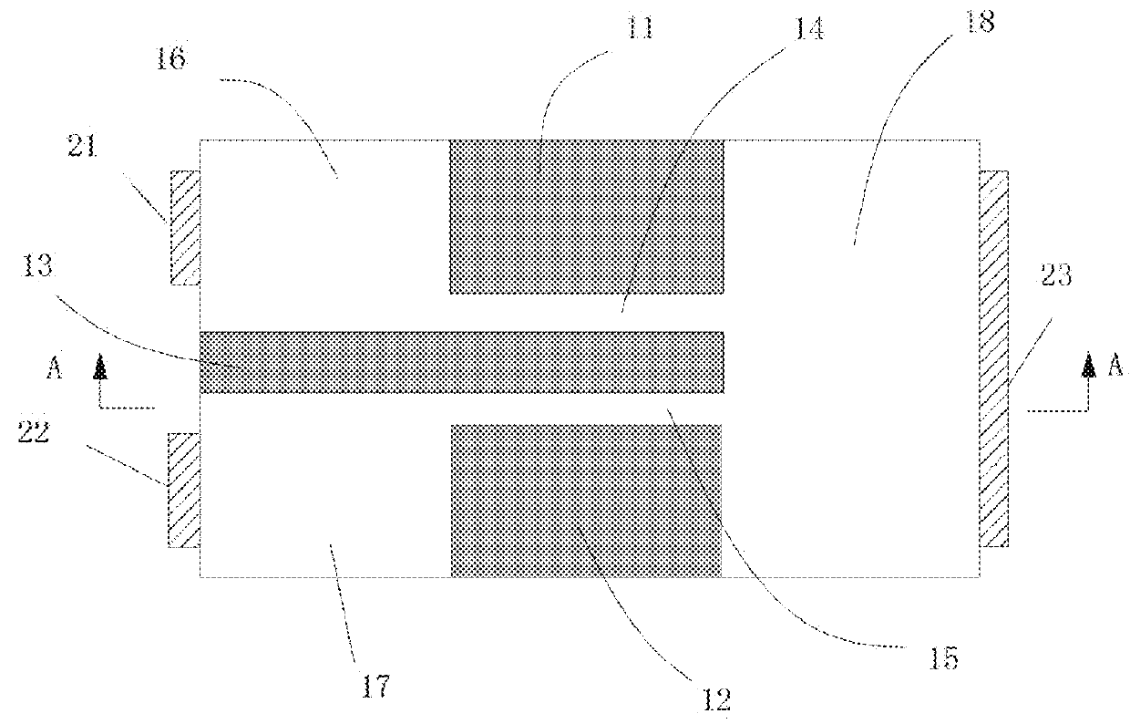
[0039]Referring to FIG. 1, this is a top plan view of the frequency multiplier based on a low dimensional semiconductor structure in this embodiment, omitting the insulating protective layer. Thus, a first insulating carving groove 11, a second insulating carving groove 12, a third insulating carving groove 13, a first inlet electrode 21, a second inlet electrode 22, and a outlet electrode 23 are visible. The third insulating carving groove 13 is inserted between the first insulating carving groove 11 and the second insulating carving groove 12. The first insulating carving groove 11 and the second insulating carving groove 12 are arranged in an opposite position. The space between the first insulating carving groove 11 and the third insulating carving groove 13 forms the first current carrying channel 14; the space between the second insulating carving groove 12 and the third insulating carving groove 13 forms the second current carrying channel 15. The area surrounded by the first...

embodiment 2

[0046]In this embodiment, the semiconductor conducting layer employs the two-dimensional semiconductor material.

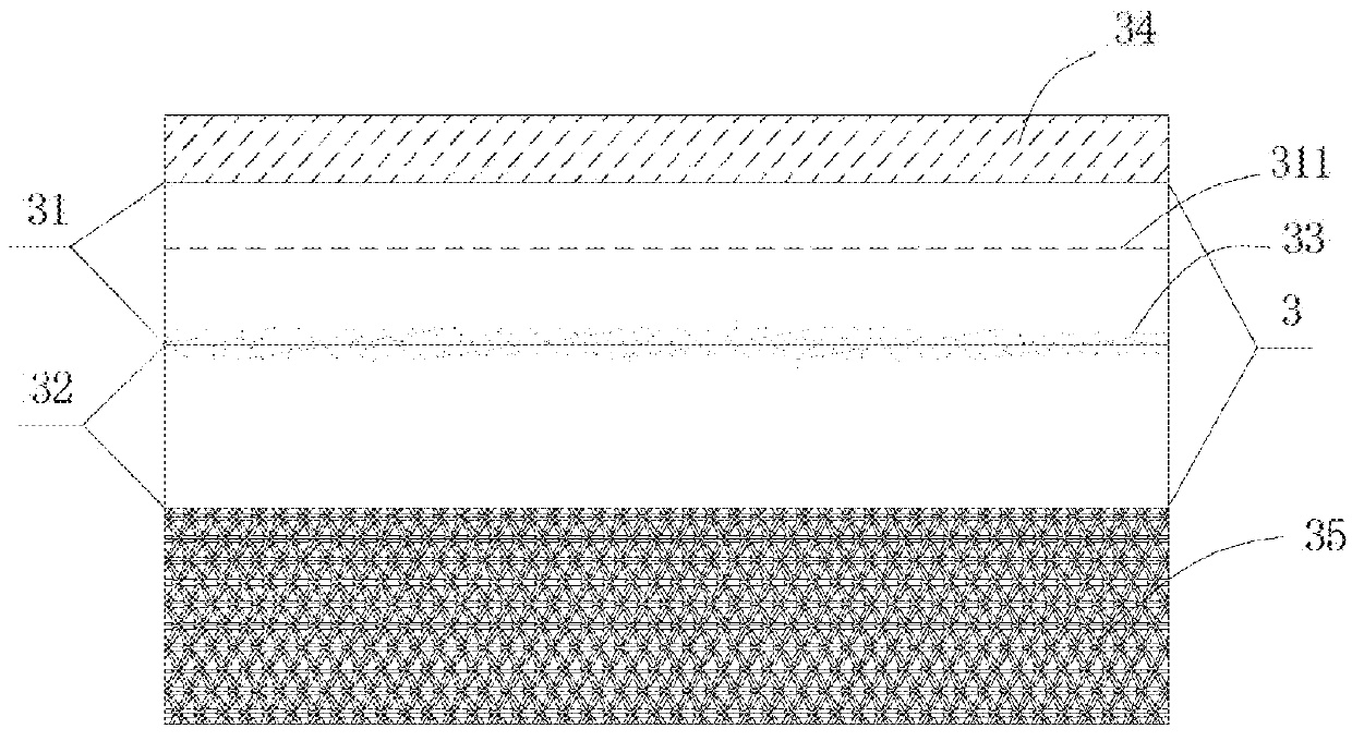
[0047]Referring to FIG. 5, this is a schematic diagram of the surface of the frequency multiplier with two-dimensional current carrying channels. The first insulating carving groove 41 and the second insulating carving groove 42 are oppositely arranged. The space between the first insulating carving groove 41 and the second insulating carving groove 42 forms the current carrying channels. The first low resistance area 45 is on one side of the first insulating carving groove 41, the current carrying channels, and the second insulating carving groove 42, and the second resistance low area 46 is on the other side. The first low resistance area 45 is connected with the second low resistance area 46 through the current carrying channel. Referring to FIG. 6, when the current carrying channel is two dimensional, the semiconductor structure of the frequency multiplier comprises th...


PUM


Abstract

A frequency multiplier based on a low dimensional semiconductor structure, including an insulating substrate layer, a semiconductor conducting layer arranged on the surface of the insulating substrate layer, an insulating protective layer arranged on the surface of the semiconductor conducting layer, an insulating carving groove penetrating the semiconductor conducting layer, an inlet electrode arranged on the side surface of the semiconductor conducting layer, and an outlet electrode arranged on the side surface corresponding to the access electrode is provided. The semiconductor conducting layer comprises two two-dimensional, quasi-one-dimensional, or one-dimensional current carrying channels near to and parallel to each other. The frequency multiplier has advantages that the structure is simple, the process is easy to implement, no extra filter circuit needs to be added, dependence on material characteristics is little, and the selection range of materials is wide.

Description

CROSS-REFERENCE TO RELATED APPLICATIONS[0001]This application claims priority to PCT Application No. PCT / CN2014 / 073996, having a filing date of Mar. 25, 2014, based on CN 201310144245.7, having a filing date of Apr. 23, 2013, the entire contents of which are hereby incorporated by reference.FIELD OF TECHNOLOGY[0002]The following relates to a frequency multiplier based on a low dimensional semiconductor structure, in particular to a frequency multiplier which needs no additional filter circuit and can work at terahertz frequencies at room temperature.BACKGROUND[0003]As semiconductor technology is developing continuously, the characteristic lengths of devices have constantly reduced from micron to the current nanometer scale; and, the corresponding material system structures used have also changed from the traditional higher dimensions (three-dimensions) to lower dimensions (two-dimensions, quasi-one-dimension and one-dimension). Devices based on the low dimensional semiconductor stru...

Claims


Application Information

Patent Timeline
IPC IPC(8): H01L29/20H03B19/14
CPCH03B19/14H01L29/2003H01L29/778
Inventor XU, KUNYUAN
Owner SOUTH CHINA NORMAL UNIVERSITY
Why Eureka
Try Eureka