Semiconductor memory devices, memory systems including the same and method of correcting errors in the same

a memory device and semiconductor technology, applied in the field of memory devices, can solve the problems of increasing the ber of memory cells in the semiconductor memory device, and achieve the effect of reducing the number of parity bits or check bits required for correcting errors and high probability of errors

Active Publication Date: 2016-03-03
SAMSUNG ELECTRONICS CO LTD
View PDF10 Cites 26 Cited by
  • Summary
  • Abstract
  • Description
  • Claims
  • Application Information

AI Technical Summary

Benefits of technology

[0040]Accordingly, errors in a codeword read from the selected memory cell row may be corrected on a per symbol basis, where two data of two adjacent memory cells are assigned to one symbol. There

Problems solved by technology

As fabrication process of the semiconductor memory devices advances and the devices become smaller

Method used


Image

  • Semiconductor memory devices, memory systems including the same and method of correcting errors in the same
  • Semiconductor memory devices, memory systems including the same and method of correcting errors in the same
  • Semiconductor memory devices, memory systems including the same and method of correcting errors in the same

Examples


Embodiment Construction

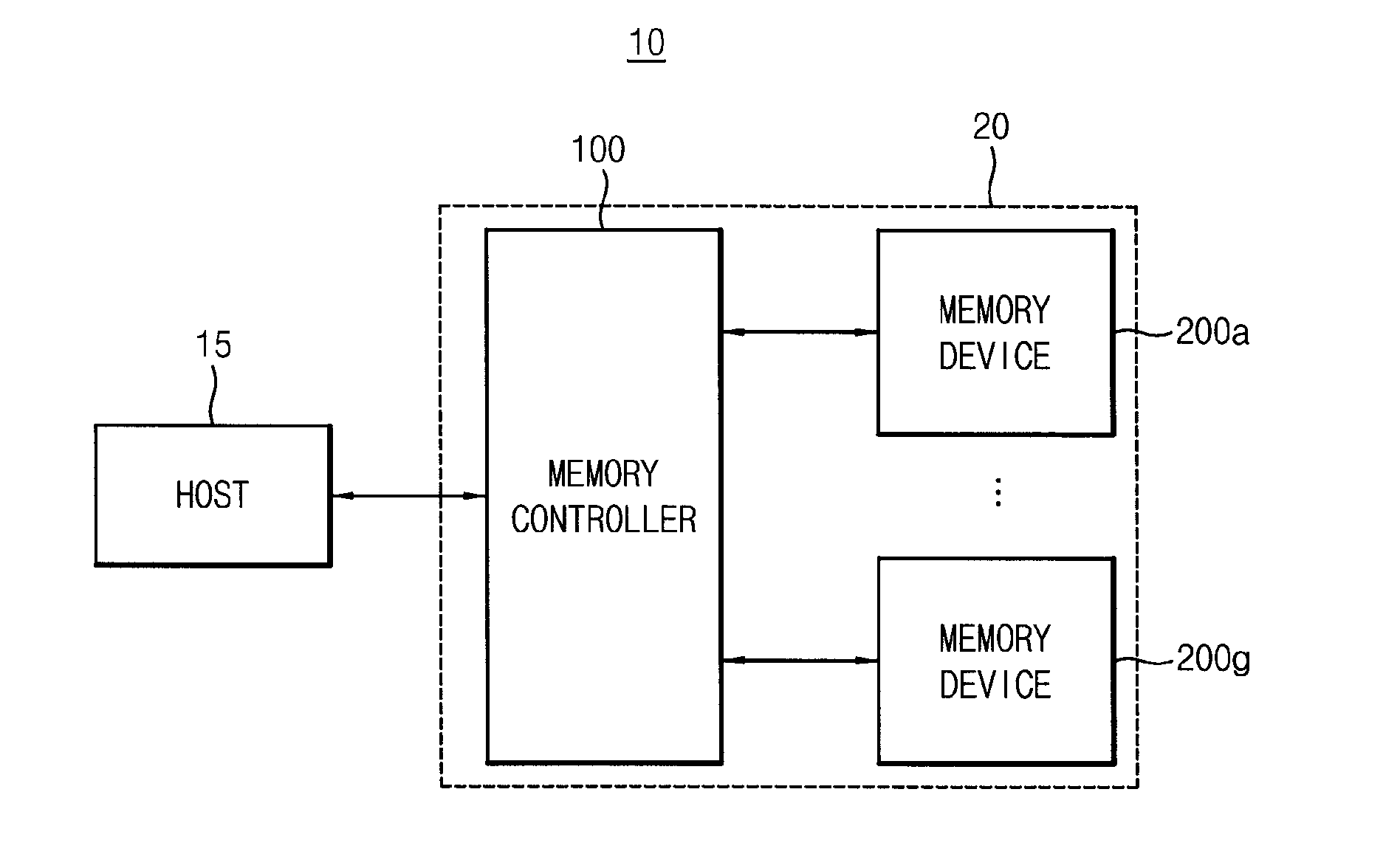
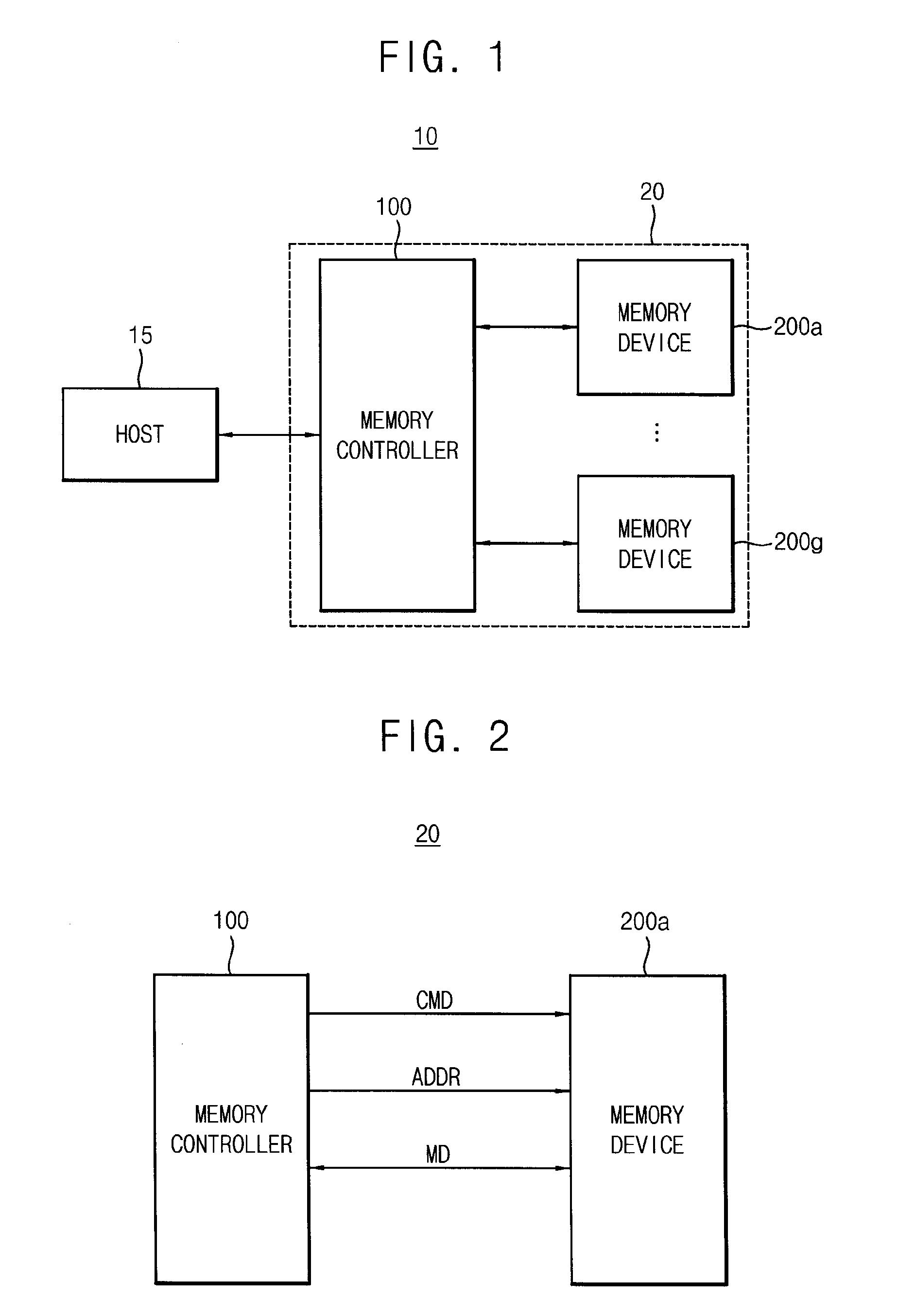
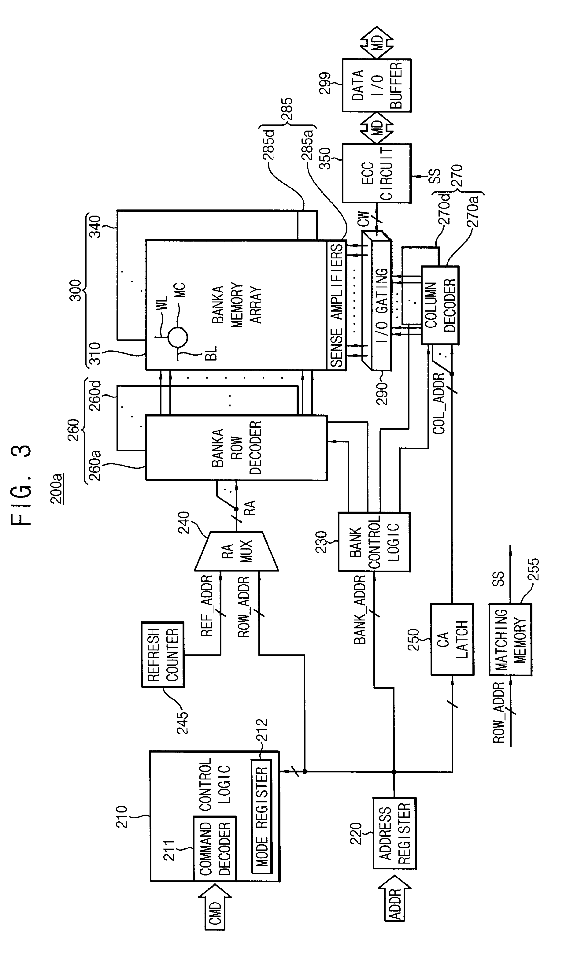
[0067]Inventive concepts will now be described more fully with reference to the accompanying drawings, in which example embodiments of are shown. These example embodiments are provided so that this disclosure will be thorough and complete, and will fully convey inventive concepts of to those skilled in the art. Inventive concepts may be embodied in many different forms with a variety of modifications, and a few embodiments will be illustrated in drawings and explained in detail. However, this should not be construed as being limited to example embodiments set forth herein, and rather, it should be understood that changes may be made in these example embodiments without departing from the principles and spirit of inventive concepts, the scope of which are defined in the claims and their equivalents. Like numbers refer to like elements throughout. In the drawings, the thicknesses of layers and regions are exaggerated for clarity.

[0068]It will be understood that, although the terms fir...


PUM


Abstract

A semiconductor memory device includes a memory cell array in which a plurality of memory cells are arranged. The semiconductor memory device includes an error correcting code (ECC) circuit configured to generate parity data based on main data, write a codeword including the main data and the parity data in the memory cell array, read the codeword from a selected memory cell row to generate syndromes, and correct errors in the read codeword on a per symbol basis based on the syndromes. The main data includes first data of a first memory cell of the selected memory cell row and second data of a second memory cell of the selected memory cell row. The first data and the second data are assigned to one symbol of a plurality of symbols, and the first memory cell and the second memory cell are adjacent to each other in the memory cell array.

Description

CROSS-REFERENCE TO RELATED APPLICATION(S)[0001]This U.S. application claims the benefit of priority under 35 USC §119 to Korean Patent Application No. 10-2014-0111225, filed on Aug. 26, 2014, in the Korean Intellectual Property Office, the contents of which are incorporated herein in their entirety by reference.BACKGROUND[0002]1. Technical Field[0003]At least one example embodiment relates to memory devices, and more particularly to semiconductor memory devices, memory systems including the same and / or methods of correcting errors in the same.[0004]2. Discussion of the Related Art[0005]Semiconductor memory devices can be divided into two categories according to whether they retain stored data when disconnected from power. These categories include volatile memory devices, which lose stored data when disconnected from power, and nonvolatile memory devices, which retain stored data when disconnected from power. Examples of volatile memory devices include static random access memory (SR...

Claims


Application Information

Patent Timeline
IPC IPC(8): G06F11/10G11C29/52
CPCG11C29/52G06F11/1068G11C29/702G11C2029/0411G11C2029/4402G06F11/1048G11C11/1659G11C11/1673G11C11/1675G11C11/1653G11C11/15
Inventor CHA, SANG-UHNCHUNG, HOI-JUSON, JONG-PILPARK, KWANG-ILJANG, SEONG-JIN
Owner SAMSUNG ELECTRONICS CO LTD
Why Eureka
Try Eureka