Light emitting diode structure

Active Publication Date: 2016-03-03
EPISTAR CORP
View PDF4 Cites 19 Cited by
  • Summary
  • Abstract
  • Description
  • Claims
  • Application Information

AI Technical Summary

Benefits of technology

[0028]Based on the abovementioned description, the LED structure of the present invention adopts the dielectric reflective layer as the reflective layer for reflecting the light emitted by the active layer, and the dielectric reflective layer connects to the contact layer and the first type doped layer with a coverage rate equal to or less than 60% fr

Problems solved by technology

However, the reflectivity of the metal reflecting layer is limited.
However, the DBR layer is made of non-conductive material, so the disposition of the DBR laye

Method used


Image

  • Light emitting diode structure
  • Light emitting diode structure
  • Light emitting diode structure

Examples


Embodiment Construction

[0035]Reference will now be made in detail to the present preferred embodiments of the invention, examples of which are illustrated in the accompanying drawings. Wherever possible, the same reference numbers are used in the drawings and the description to refer to the same or like parts.

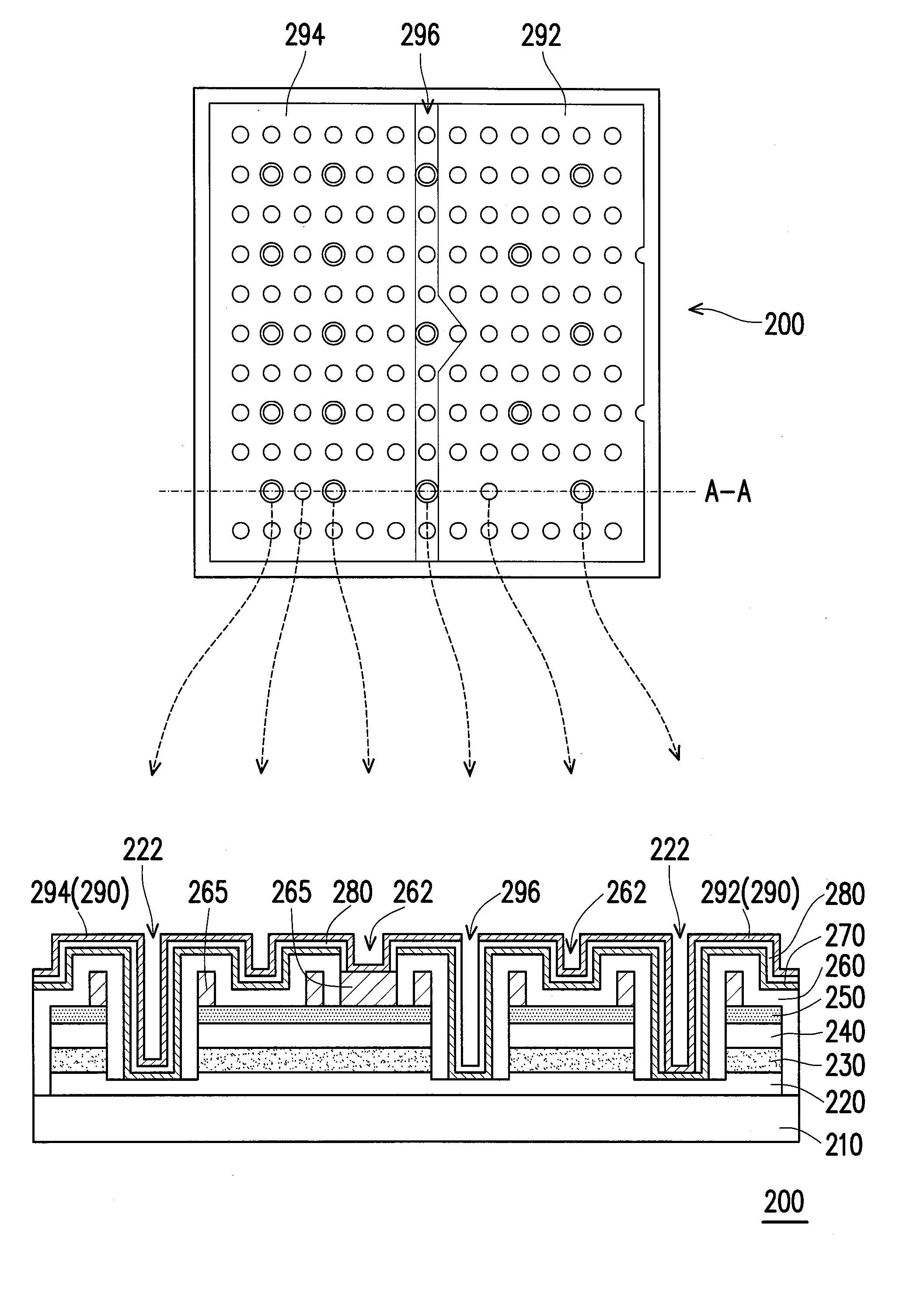
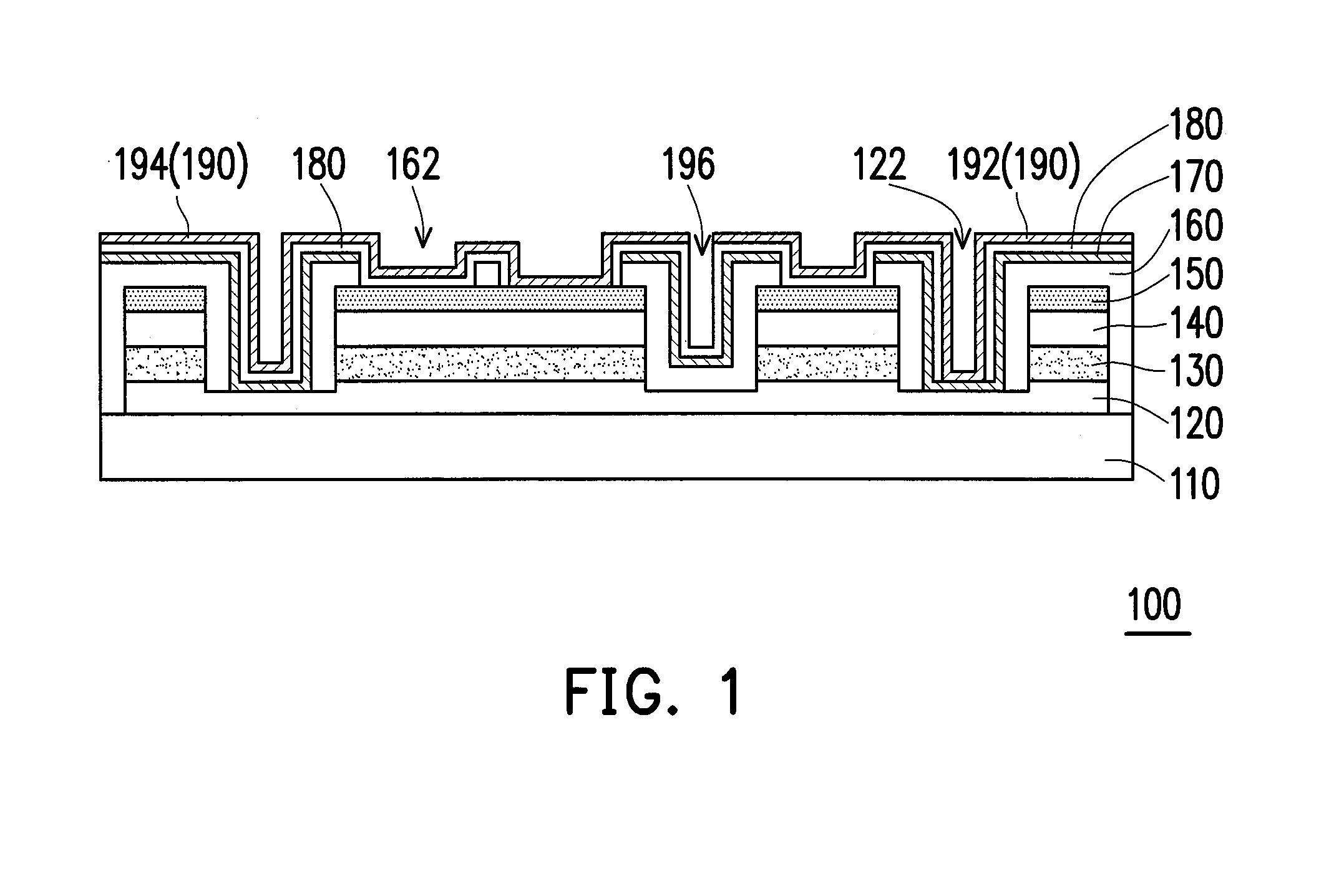
[0036]FIG. 1 illustrates a schematic cross-sectional view of a LED structure according to an embodiment of the invention. Referring to FIG. 1, in the present embodiment, a GaN based light emitting diode (LED) structure 100 may be a flip-chip type LED structure which includes a stacked semiconductor layer 120, 130, 140, a contact layer 150 and a dielectric reflective layer 160. The stacked semiconductor layer includes a first type doped layer 120, an active layer 130 and a second type doped layer 140. The active layer 130 is disposed between the first type doped layer 120 and the second type doped layer 140. In the present embodiment, the first type doped layer 120, the active layer 130 and the second...


PUM


Abstract

A light emitting diode (LED) structure including a stacked semiconductor layer, a contact layer and a dielectric reflective layer is provided. The stacked semiconductor layer includes a first type doped layer, a second type doped layer and an active layer disposed between the first type doped layer and the second type doped layer, wherein the first type doped layer, the active layer and the second type doped layer are penetrated by a plurality of recesses. The contact layer is disposed on the second type doped layer. The dielectric reflective layer is disposed on the contact layer and extended into the recesses to connect the contact layer and the first type doped layer with a coverage rate equal to or less than 60% from a top view of the LED structure.

Description

BACKGROUND OF THE INVENTION[0001]1. Field of the Invention[0002]The present invention generally relates to a semiconductor structure. More particularly, the present invention relates to light emitting diode structure.[0003]2. Description of Related Art[0004]A light emitting diode (LED) has the characteristics of high efficiency, long lifespan, etc. and thus the LED light source has been widely applied. The light-emitting diode (LED) formed by semiconductor material of the compound of the group III-V elements is a wide band-gap luminous component, which emits the light covering all wavebands of visible light. In recent years, following the progress towards high-chroma and extreme-brightness, LEDs have gained broader applications fields, such as mega-size outdoor display boards and traffic lights, and would even substitute tungsten lamps and mercury lights to become a future lighting source with energy-saving and environmentally friendly advantages.[0005]In a conventional GaN based LE...

Claims


Application Information

Patent Timeline
IPC IPC(8): H01L33/46H01L33/36H01L33/62
CPCH01L33/46H01L33/36H01L33/62H01L33/382H01L33/387H01L33/405H01L33/08
Inventor YANG, CHENG-KUANGFENG, HUI-CHINGHSU, CHIEN-PINYU, KUO-HUIPAN, SHYI-MING
Owner EPISTAR CORP
Why Eureka
Try Eureka