This helps you quickly interpret patents by identifying the three key elements:
Problems solved by technology
Method used
Benefits of technology
[0047]Alternatively, a transistor having normally-off electrical characteristics can be provided. Alternatively, a transistor having a low leakage current in an off state can be provided. Alternatively, a transistor having a small subthreshold swing value can be provided. Alternatively, a transis
Problems solved by technology
For example, a display device to which a transistor including an oxi
Method used
Image
Click on the blue label to locate the original text in one second.
Reading with bidirectional positioning of images and text.
Examples
Example
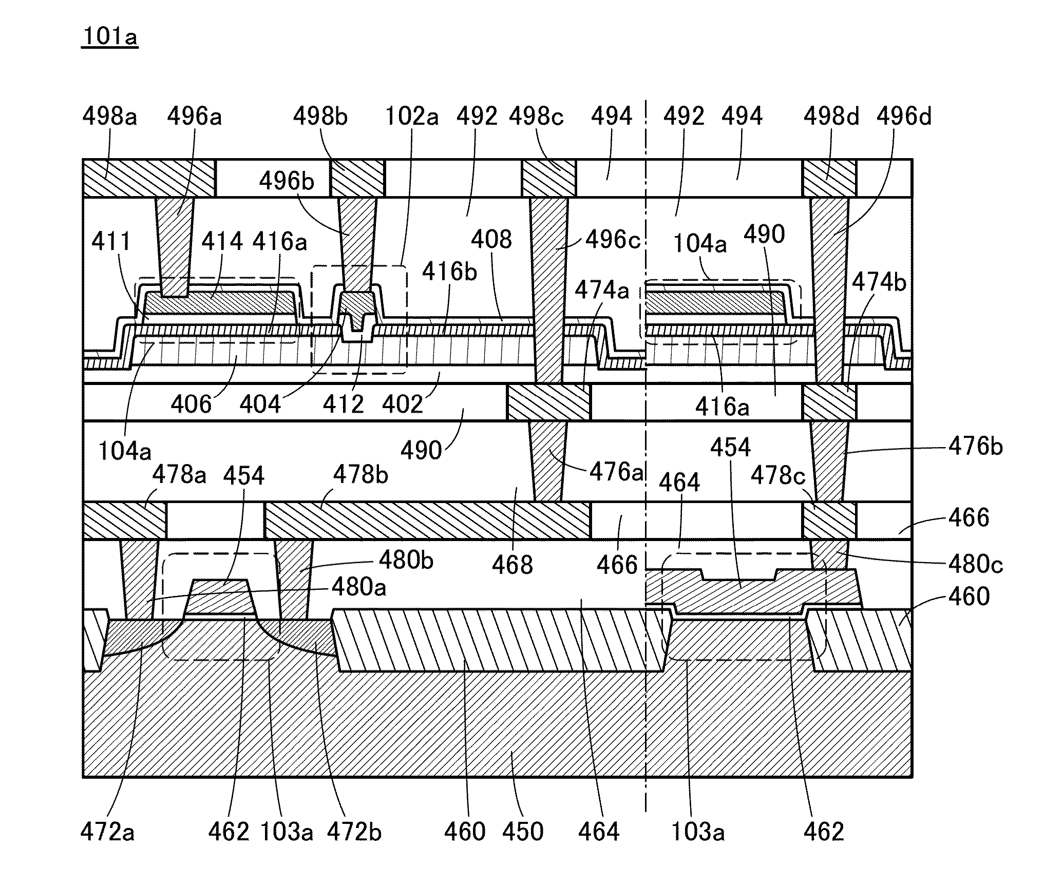
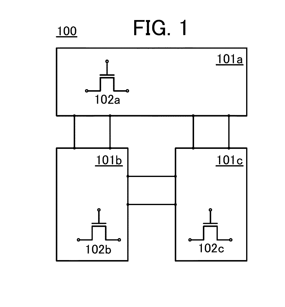
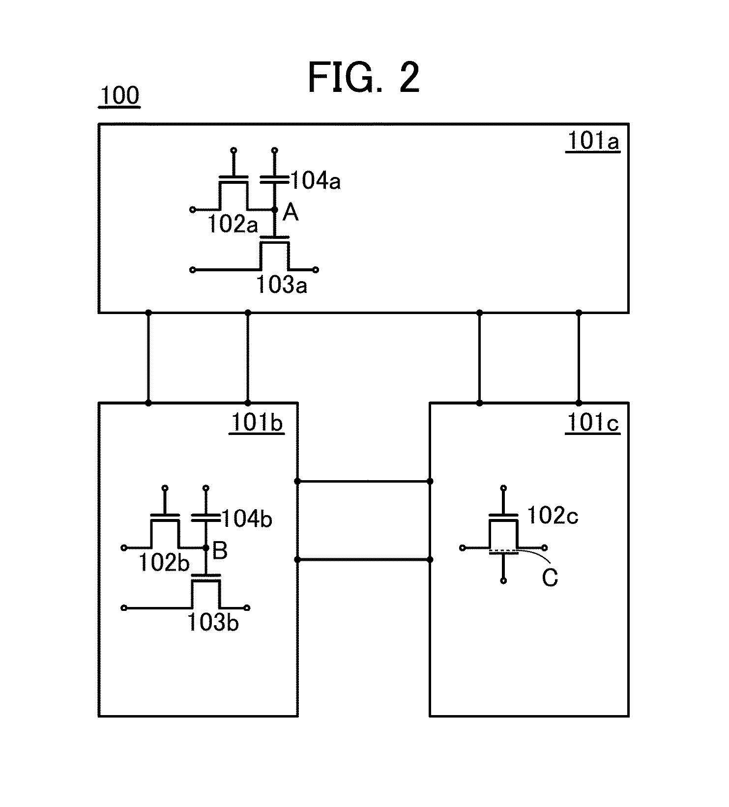
[0074]Embodiments of the present invention will be described in detail with the reference to the drawings. However, the present invention is not limited to the following description, and it is easily understood by those skilled in the art that modes and details disclosed herein can be modified in various ways. Furthermore, the present invention is not construed as being limited to description of the following embodiments. In describing structures of the invention with reference to the drawings, common reference numerals are used for the same portions in different drawings. Note that the same hatched pattern is applied to similar parts, and the similar parts are not especially denoted by reference numerals in some cases.
[0075]Note that the size, the thickness of films (layers), or regions in drawings is sometimes exaggerated for clarification.
[0076]In this specification, the terms “film” and “layer” can be interchanged with each other.
[0077]A voltage usually refers to a potential dif...
PUM
Abstract
A semiconductor device that includes transistors with different threshold voltages is provided. Alternatively, a semiconductor device including a plurality of kinds of circuits and transistors whose electrical characteristics are different between the circuits is provided. The semiconductor device includes a first transistor and a second transistor. The first transistor includes an oxide semiconductor, a conductor, a first insulator, a second insulator, and a third insulator. The conductor has a region where the conductor and the oxide semiconductor overlap with each other. The first insulator is positioned between the conductor and the oxide semiconductor. The second insulator is positioned between the conductor and the first insulator. The third insulator is positioned between the conductor and the second insulator. The second insulator has a negatively charged region.
Description
BACKGROUND OF THE INVENTION[0001]1. Field of the Invention[0002]The present invention relates to, for example, a semiconductor, a transistor, and a semiconductor device. The present invention relates to, for example, a method for manufacturing a semiconductor, a transistor, and a semiconductor device. The present invention relates to, for example, a semiconductor, a display device, a light-emitting device, a lighting device, a power storage device, a memory device, a processor, and an electronic device. The present invention relates to a method for manufacturing a semiconductor, a display device, a liquid crystal display device, a light-emitting device, a memory device, and an electronic device. The present invention relates to a driving method of a semiconductor device, a display device, a liquid crystal display device, a light-emitting device, a memory device, and an electronic device.[0003]Note that one embodiment of the present invention is not limited to the above technical fie...
Claims
Application Information
Patent Timeline
Application Date:The date an application was filed.
Publication Date:The date a patent or application was officially published.
First Publication Date:The earliest publication date of a patent with the same application number.
Issue Date:Publication date of the patent grant document.
PCT Entry Date:The Entry date of PCT National Phase.
Estimated Expiry Date:The statutory expiry date of a patent right according to the Patent Law, and it is the longest term of protection that the patent right can achieve without the termination of the patent right due to other reasons(Term extension factor has been taken into account ).
Invalid Date:Actual expiry date is based on effective date or publication date of legal transaction data of invalid patent.