Semiconductor device having metal gate and manufacturing method thereof

a technology of semiconductor devices and metal gates, which is applied in the direction of semiconductor devices, electrical devices, transistors, etc., can solve the problems of metal gate seams left in metal gates, deterioration of electrical performance of semiconductor devices having metal gates, and opening width, etc., to achieve superior gap-filling results, easy formation, and large opening width

Active Publication Date: 2016-03-10
UNITED MICROELECTRONICS CORP
View PDF2 Cites 40 Cited by
  • Summary
  • Abstract
  • Description
  • Claims
  • Application Information

AI Technical Summary

Benefits of technology

[0009]According to the method for manufacturing the semiconductor device having the metal gates provided by the present invention, the taper top of the first work function metal layer is obtained by performing the two-step etching process, and the taper top of the first work function metal layer provides a larger opening width, thus the metal layers are more easily formed in the gate trench. Consequently, the semiconductor device having the metal gates provided by the present invention has the advantage of superior gap-filling result and improved reliability.

Problems solved by technology

Briefly speaking, when the line width of the semiconductor device is reduced, the opening width of the gate trench is consequently reduced, and thus it is difficult to fill the gate trench with the metals, it even causes a seam left in the metal gate after forming the metal layers in the gate trench.
Eventually, the electrical performance of the semiconductor device having the metal gate is deteriorated.

Method used


Image

  • Semiconductor device having metal gate and manufacturing method thereof
  • Semiconductor device having metal gate and manufacturing method thereof
  • Semiconductor device having metal gate and manufacturing method thereof

Examples


Embodiment Construction

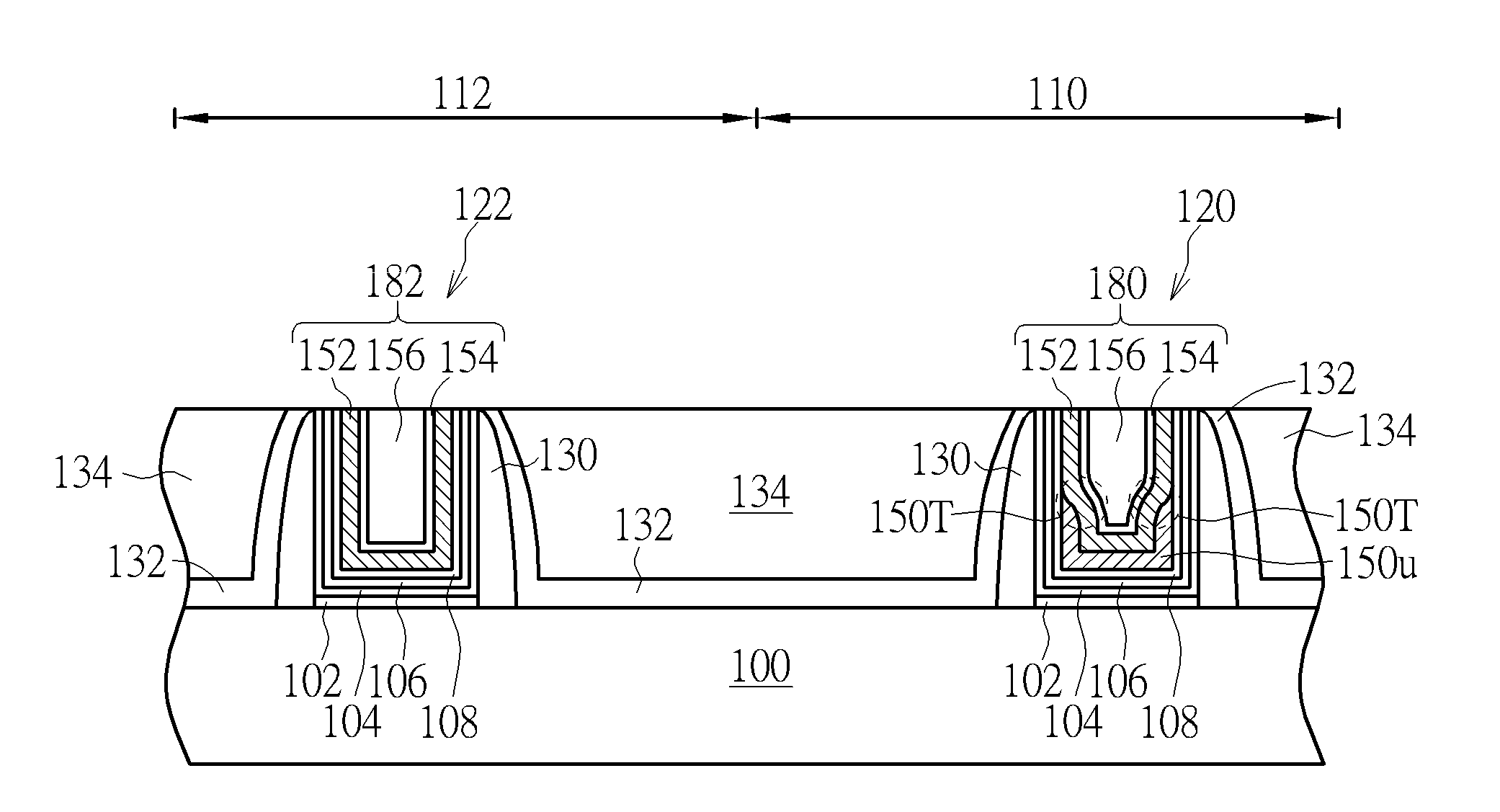
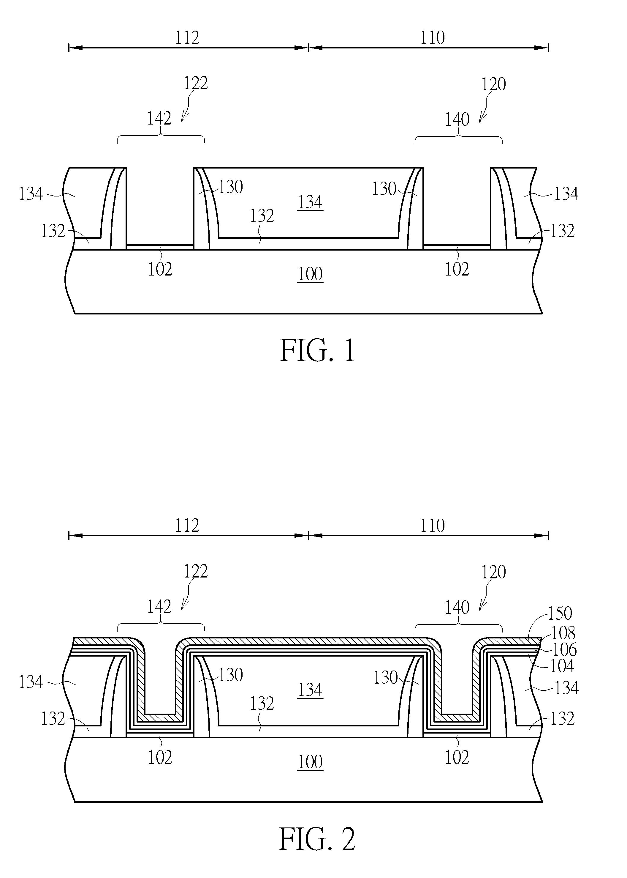
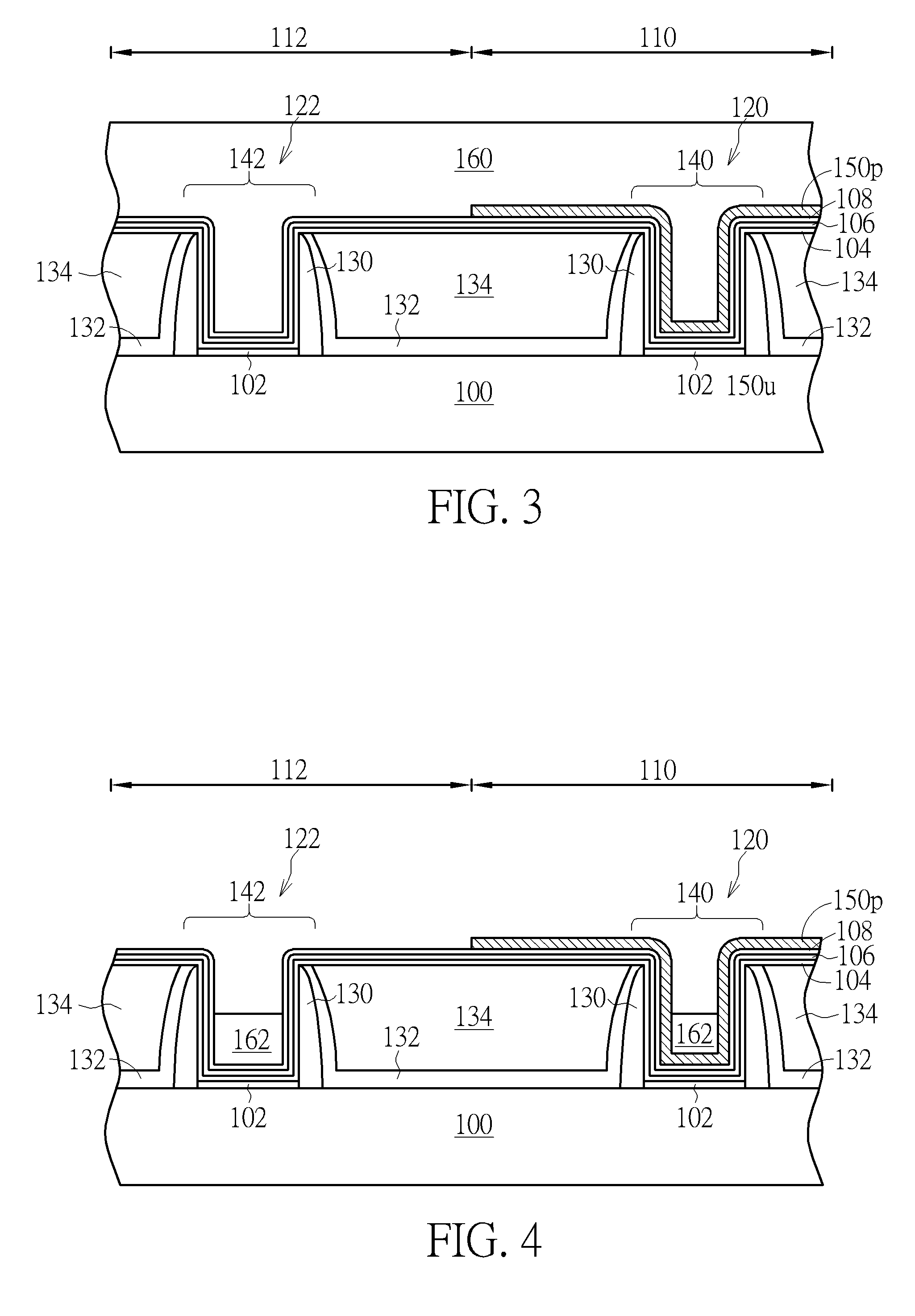
[0019]Please refer to FIGS. 1-8, which are drawings illustrating a method for manufacturing a semiconductor device having metal gates provided by a preferred embodiment of the present invention. As shown in FIG. 1, the preferred embodiment first provides a substrate such as a silicon substrate, a silicon-containing substrate, or a silicon-on-insulator (hereinafter abbreviated as SOI) substrate. The substrate includes a plurality of shallow trench isolations (hereinafter abbreviated as STIs) (not shown), and the STIs are used to define a plurality of active regions for accommodating p-typed transistors and n-typed transistors and to provide electrical isolation. In the preferred embodiment, a semiconductor layer such as a fin structure involved in fin field effect transistor (FinFET) approach is provided. The fin structure as shown in FIG. 1 can be formed by patterning a single crystalline silicon layer of a SOI substrate or a bulk silicon substrate. And the fin structure is taken as...


PUM

PropertyMeasurementUnit
include angleaaaaaaaaaa
work functionaaaaaaaaaa

Abstract

A semiconductor device having metal gate includes a substrate, a first metal gate positioned on the substrate, and a second metal gate positioned on the substrate. The first metal gate includes a first work function metal layer, and the first work function metal layer includes a taper top. The second metal gate includes a second work function metal layer. The first work function metal layer and the second work function metal layer are complementary to each other.

Description

BACKGROUND OF THE INVENTION[0001]1. Field of the Invention[0002]The invention relates to a semiconductor device having metal gate and manufacturing method thereof, and more particularly, to a semiconductor device having metal gate and manufacturing method capable of providing superior gap-filling result.[0003]2. Description of the Prior Art[0004]With a trend toward scaling down the size of the semiconductor device, work function metals are used to replace the conventional polysilicon gate to be the control electrode that competent to the high dielectric constant (herein after abbreviated as high-k) gate dielectric layer. The conventional metal gate methods are categorized into the gate first process and the gate last process. Among the two main processes, the gate last process is able to avoid processes of high thermal budget and to provide wider material choices for the high-k gate dielectric layer and the metal gate, and thus the gate last process gradually replaces the gate first...

Claims


Application Information

Patent Timeline
Patent Type & Authority Applications(United States)
IPC IPC(8): H01L29/423H01L27/088H01L29/40H01L29/51
CPCH01L29/42376H01L29/401H01L29/512H01L27/0883H01L21/823842H01L27/092H01L29/165H01L29/4966H01L29/513H01L29/66545H01L29/66628
Inventor LU, CHIA-LINCHEN, CHUN-LUNGLIAO, KUN-YUANCHANG, FENG-YI
Owner UNITED MICROELECTRONICS CORP
Why Eureka
Try Eureka