

Semiconductor device and method of manufacturing the same
a semiconductor and semiconductor technology, applied in the direction of capacitors, basic electric elements, electrical appliances, etc., can solve the problems of reducing the area occupied by memory cell capacitors, degrading the charge holding property of drams, and reducing the capacitance value of each capacitor, etc., to achieve small opening width, large opening width, and high yield
- Summary
- Abstract
- Description
- Claims
- Application Information
AI Technical Summary
Benefits of technology
Problems solved by technology
Method used
Image

Examples
first embodiment
>
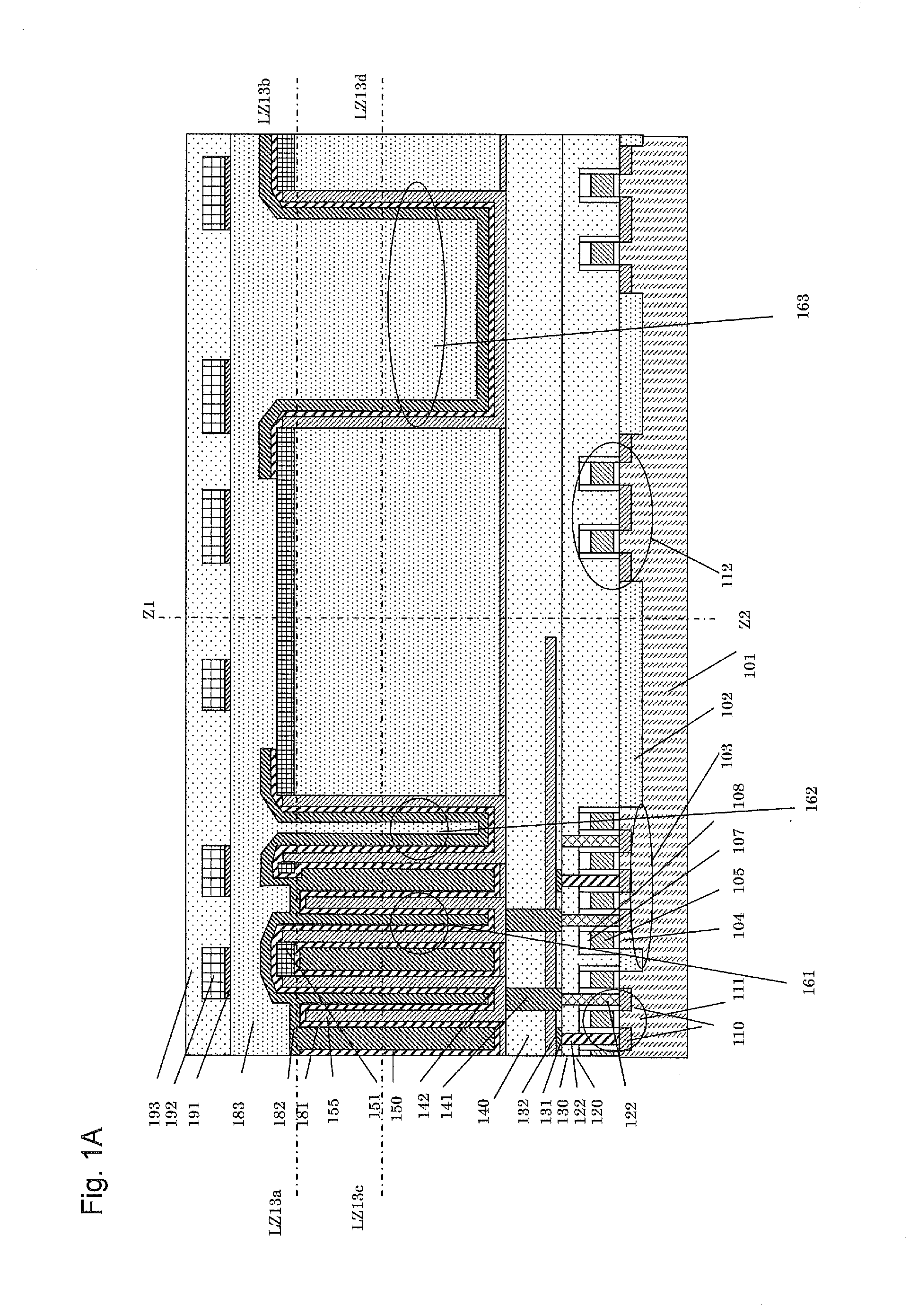
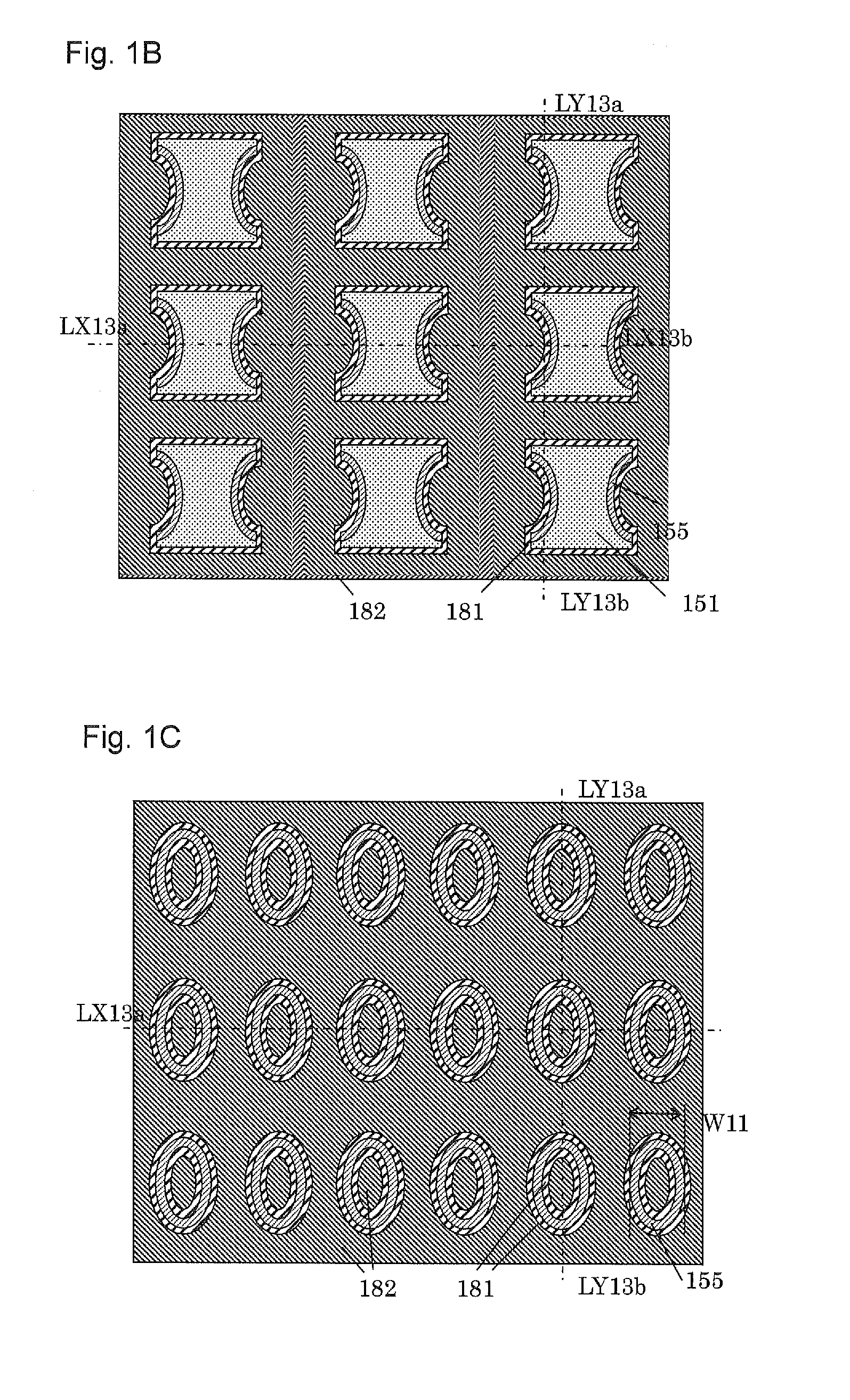
[0051]FIG. 2 is a conceptual drawing showing a structure of a semiconductor device according to a first embodiment, wherein FIG. 2(a) is a diagram showing an appearance of a semiconductor device as a whole, FIG. 2(b) is an enlarged view of a memory cell array, FIG. 2(c) is an enlarged view of a pattern of memory cell capacitors, and FIG. 2(d) is an enlarged view of a lithography mark portion.
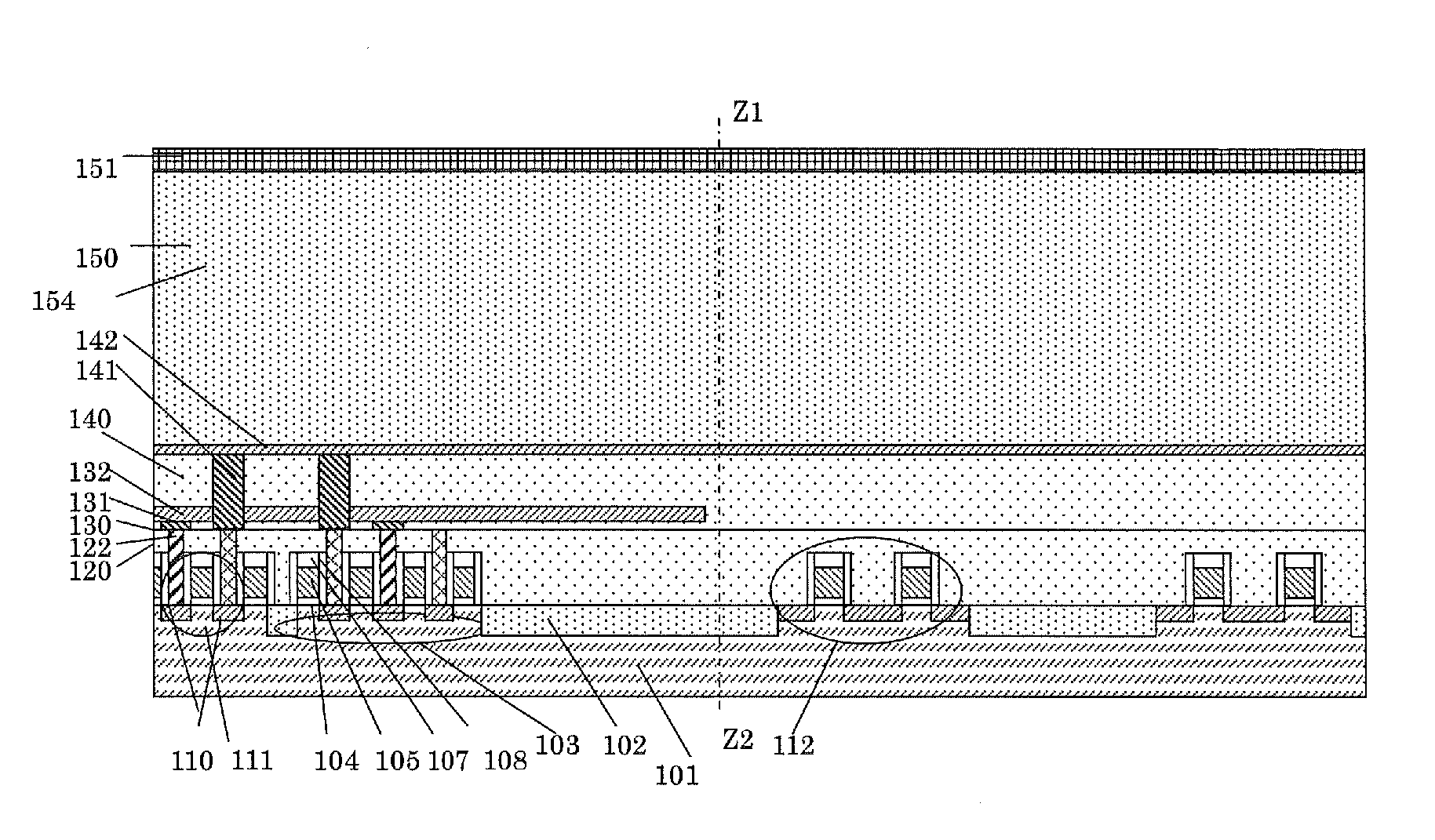
[0052]As shown in FIG. 2(a), scribe line 17 encloses the periphery of semiconductor chip 13 and element region 18 is formed inside scribe line 17. Memory cell arrays 14, array circuits 15, and peripheral circuit 16 are formed in element region 18; each of memory cell arrays 14 includes memory cells arranged therein in array form, and array circuits 15 configured to drive memory cell arrays 14. On the other hand, lithography marks such as lithography marks 163 and second lithography marks 164 are formed on scribe line 17. Although, in a first embodiment, the lithography marks are formed in the s...
second embodiment
[0095]In a second embodiment, a manufacturing method according to a first embodiment is partly changed. A method of manufacturing a semiconductor device according to a second embodiment will be described with reference to FIGS. 4A and 4B. FIGS. 4A and 4B are vertical sectional views showing a structure of memory cells during respective manufacturing steps, which are taken across line LX13a-LX13b in FIG. 10.
4A>
[0096]Steps shown in FIGS. 3A to 3E for a first embodiment are carried out. Subsequently, exposed storage electrode conductive film 155 is etched.
4B>
[0097]A step shown in FIG. 3F for a first embodiment is carried out to leave photo resist film 172 and antireflection film 171 in a large capacitor portion.
[0098]Storage electrode conductive film 155 has already been etched away. Thus, capacitor beam insulating film 151 is etched by a step shown in FIG. 3G for a first embodiment. Thereafter, steps shown in FIG. 3H and the subsequent figures for a first embodiment are carried out to...
third embodiment
[0099]In a third embodiment, a manufacturing method according to a first or second embodiment is partly changed. A method of manufacturing a semiconductor device according to a third embodiment will be described with reference to FIGS. 5A and 5B. FIGS. 5A and 5B are vertical sectional views showing the structure of memory cells during the respective manufacturing steps, which are taken across line LX13a-LX13b in FIG. 10.
5A>
[0100]Steps shown in FIGS. 3A to 3E for a first embodiment and a step shown in FIG. 4A for a second embodiment are carried out. Subsequently, exposed capacitor beam insulating film 151 is etched away.
5B>
[0101]A step shown in FIG. 3F for a first embodiment is carried out to leave photo resists film 172 and antireflection film 171 in a large capacitor portion. At this time, the memory cell has substantially the same sectional shape as that of the structure shown in FIG. 3G for a first embodiment.
[0102]Steps shown in FIG. 3H and the subsequent figures for a first emb...
PUM
 Abstract
Description
Claims
Application Information