
Gate driver for isolated input switching element

Active Publication Date: 2016-03-10
MAPS
View PDF4 Cites 4 Cited by
  • Summary
  • Abstract
  • Description
  • Claims
  • Application Information

AI Technical Summary

Benefits of technology

The present invention introduces a new method to improve the efficiency of a gate driver by using a capacitor coupled gate driver, specifically a capacitor coupled charges recycle gate driver. This method increases overall efficiency by reducing the gate drive loss while also increasing the conduction loss. This efficiency improvement is especially useful in applications that perform zero-voltage switching and drives high-speed switching devices.

Problems solved by technology

In the case where the driving frequency is low, although gate drive loss is usually negligible compared to conduction loss caused by ON resistance Rdson of the MOSFET, the gate drive loss increases with the rise of the frequency, which means no matter how much Rdosn of the switch is improved, it is not possible to implement a system that has a good efficiency.

Method used


Image

  • Gate driver for isolated input switching element
  • Gate driver for isolated input switching element
  • Gate driver for isolated input switching element

Examples


Embodiment Construction

[0030]The above and further aspects of the present invention will be more clearly understood through the accompanying drawings, in which exemplary embodiments of the invention are shown. Hereinafter, the exemplary embodiments are provided to describe the invention in detail such that the invention can be embodied and fully understood by those skilled in the art.

[0031]FIG. 4 is a graph showing a gate driving voltage and ON resistance of MOSFET.

[0032]FIG. 4 is a graph showing ON resistances Rdson of MOSFET according to a gate driving voltage of a 20V lateral double diffused MOS (LDMOS). The X-axis represents a gate driving voltage [V] and the Y-axis represents ON voltage of MOSFET, i.e., Rdson [mOhm]. If the threshold voltage of the 20V LDMOS is set at about 0.8 V, and when the 20V LDMOS is driven above 2 V, a desired ON characteristic can be achieved. In addition, as a gate voltage is increased, Rdson decreases, but not drastically; and even when the voltage is increased, there is on...


PUM


Abstract

A gate driver driving a switching device is disclosed. The gate driver includes a capacitor which is coupled to the input of the switching device. The gate drive power consumption is reduced by this additional capacitor.

Description

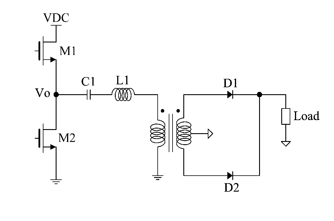
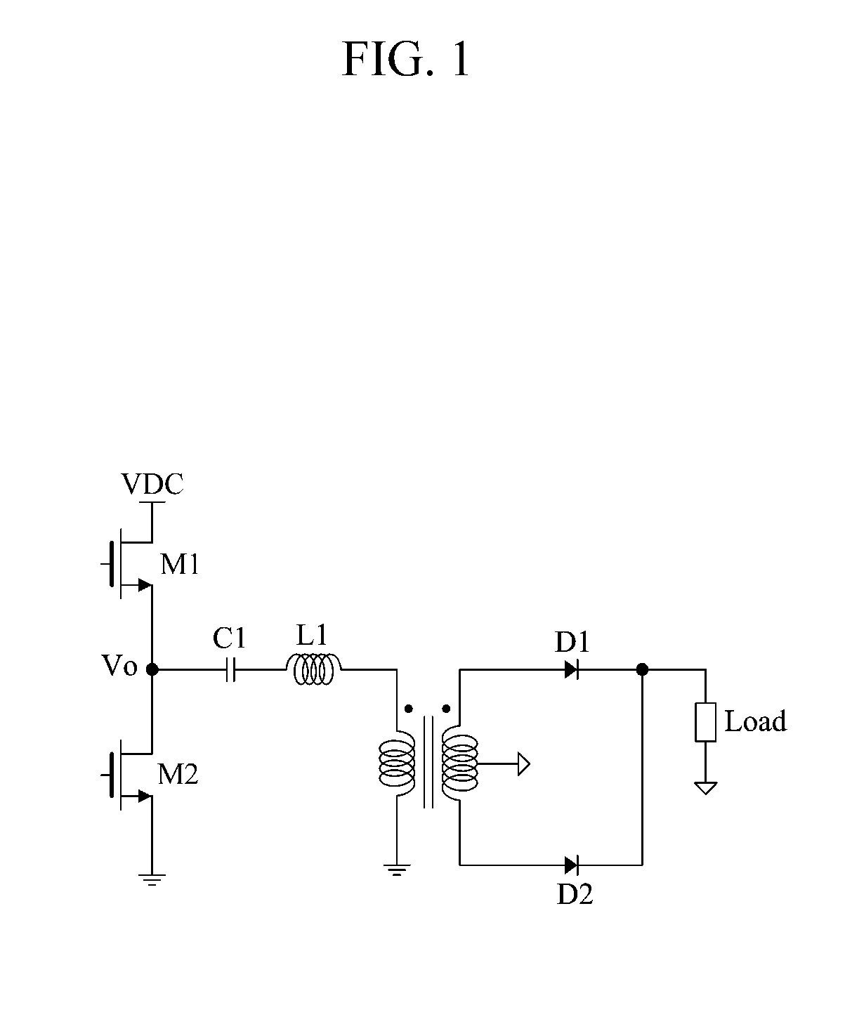
TECHNICAL FIELD[0001]The present invention relates to a gate driver for switching device, and more particularly, to a gate driver for improving driving efficiency of a switching device.BACKGROUND ART[0002]FIG. 1 is a diagram illustrating an inductor-inductor-capacitor (LLC) resonant inverter circuit consisting of conventional MOSFET switches.[0003]In the LLC resonant inverter circuit as shown in FIG. 1, MOSFET switch M1 and MOSFET switch M2 are alternately switched to supply energy to the load. In this case, if M1 and M2 are driven at a switching frequency which is higher than a resonant frequency that is determined by an inductor L1, a capacitor C1, and a magnetizing inductance, the switches can be turned ON when the drain-source voltage of either M1 or M2 is almost zero. Such an operation is referred to as a “zero-voltage switching (ZVS)”. By performing a ZVS operation, not only can switching loss of switches be minimized, but also electromagnetic interference can be reduced.[0004...

Claims


Application Information

Patent Timeline
IPC IPC(8): H03K17/16
CPCH03K17/162H03K2217/0036H03K17/687
Inventor HWANG, JONG-TAESHIN, HYUN-ICKJEON, SANG-ORHEE, JOON
Owner MAPS
Learn More