
Three-level power conversion circuit

A power conversion, three-level technology, applied in output power conversion devices, high-efficiency power electronic conversion, conversion of AC power input to DC power output, etc., to reduce costs and reduce conduction losses.

Active Publication Date: 2020-08-25
FUJI ELECTRIC CO LTD
View PDF6 Cites 0 Cited by
  • Summary
  • Abstract
  • Description
  • Claims
  • Application Information

AI Technical Summary

Problems solved by technology

[0013] It is recognized that the above requirements are conflicting requirements that focus on either cost or efficiency, which has been difficult to resolve in the past

Method used


Image

  • Three-level power conversion circuit
  • Three-level power conversion circuit
  • Three-level power conversion circuit

Examples


Embodiment 1

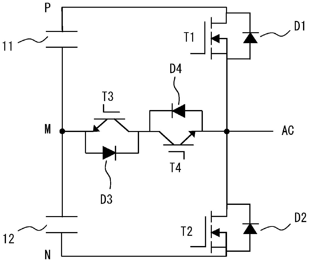
[0029] figure 2 It is a diagram showing an example when the three-level power conversion circuit according to the embodiment of the present invention is realized by a T-type three-level inverter.

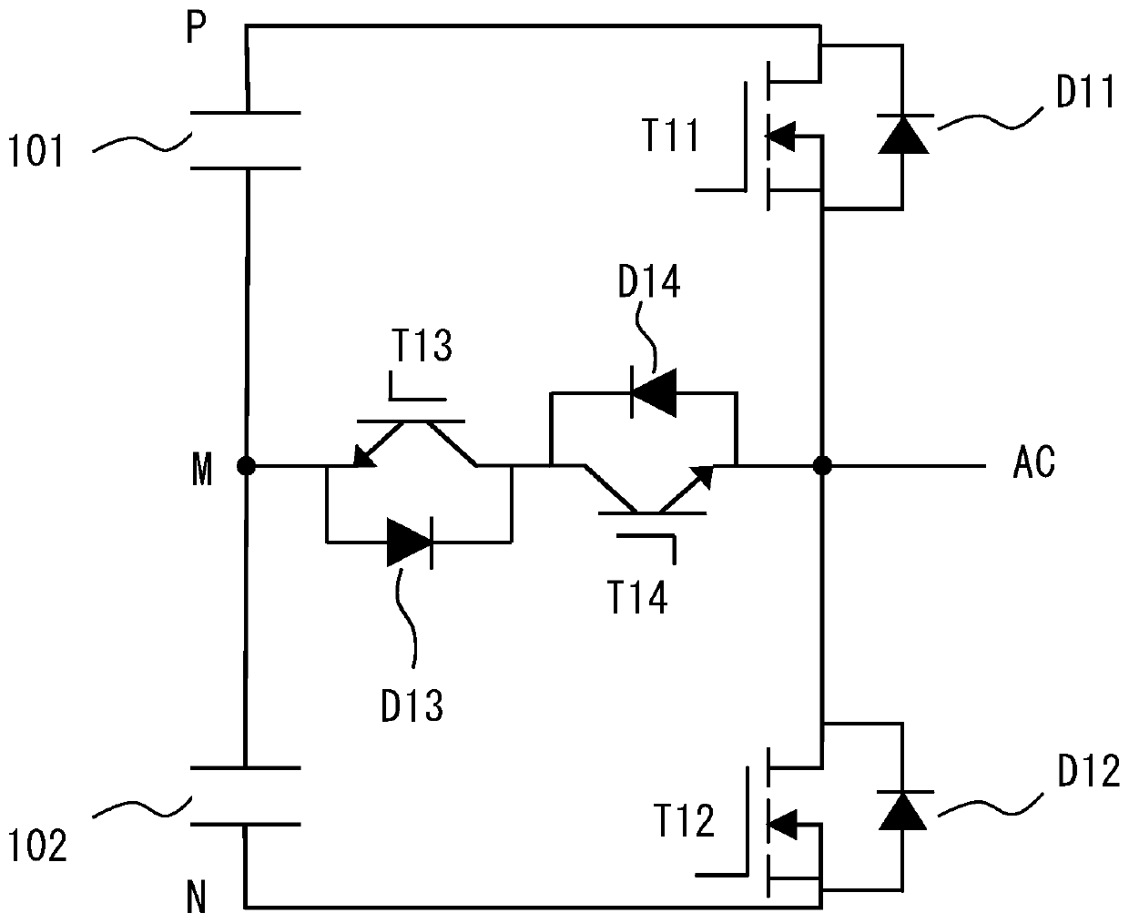
[0030] figure 2 The T-type three-level inverter shown is the same as the above figure 1 The T-type three-level inverter in the conventional example shown is the same, and the two semiconductor switching elements (such as MOSFET: Metal Oxide Semiconductor Field Effect) connected in series between the DC high potential terminal P and the DC low potential terminal N are the same. Transistor, Metal Oxide Semiconductor Field Effect Transistor) are connected, and then the connection point of the above two semiconductor switching elements is connected to the AC output terminal, and the DC high potential side P and the DC low potential side N are constituted relative to the intermediate potential (DC Neutral point) Terminal M is symmetrical.

[0031] Among them, between the AC output t...

Embodiment 2

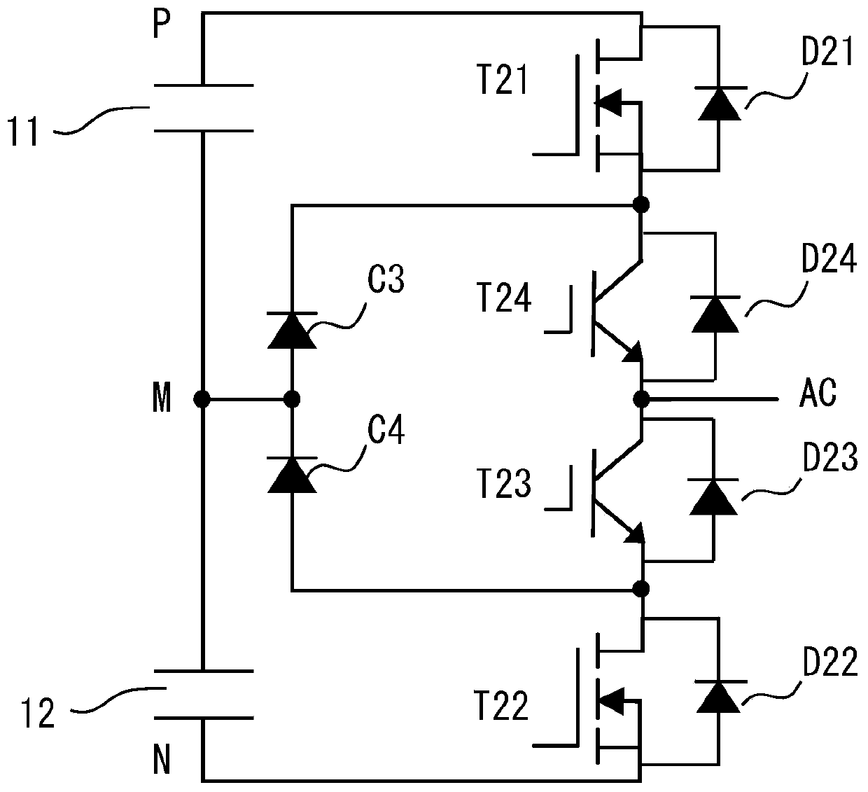
[0046] image 3 It is a diagram showing an example when the three-level power conversion circuit according to the embodiment of the present invention is realized by an I-type three-level inverter.

[0047] image 3 The shown I-type three-level inverter according to the embodiment of the present invention is the same as the I-type three-level inverter in the above-mentioned conventional example, and it uses four semiconductor switching elements in the form of MOSFET-IGBT-IGBT-MOSFET In this way, it is connected in series between the DC high potential terminal P and the DC low potential terminal N to form a four-series connection, and the connection point of the four-series connection divided into two semiconductor switching elements is connected to the AC output terminal, and the four-series connection Clamping diodes C3 and C4 are connected between each connection point of two series-connected semiconductor switching elements divided into two pairs and the intermediate potent...


PUM


Abstract

A three-level power conversion circuit. Connect the two semiconductor switching elements connected in series between the DC high potential terminal (P) and the DC low potential terminal (N), and then connect the connection point of the two semiconductor switching elements to the AC output terminal, and connect the DC high potential The side (P) and the DC low potential side (N) are configured symmetrically with respect to the intermediate potential (DC neutral point) terminal (M). Among them, a bidirectional switch configured by connecting two semiconductor switching elements (for example, IGBTs) in opposite directions is connected between the AC output terminal and the intermediate potential terminal (M). Accordingly, the current capacity of the diodes (for example, made of SiC) (D3 and D4) is smaller than that of the semiconductor switching elements (for example, made of Si) (T3 and T4).

Description

technical field [0001] The present invention relates to a three-level power conversion circuit (for example, an inverter) in which SiC (Silicon Carbide: silicon carbide) elements and Si (Silicon: silicon) elements are combined. Background technique [0002] As shown in the following patent documents 1 and 2, the following three-level inverters have been known in the past: using a two-level inverter capable of obtaining two-level outputs to obtain three-level outputs can reduce the output voltage. Contains higher harmonics. which is. [0003] In a first example of a conventional three-level inverter shown in FIGS. 11 and 16 of Patent Document 1 below, two semiconductor switches connected in series between a DC high potential terminal P and a DC low potential terminal N The components (such as IGBT: Insulated Gate Bipolar Transistor, insulated gate bipolar transistor) are connected, and then the connection point of the two semiconductor switching elements is connected to the...

Claims


Application Information

Patent Timeline
Patent Type & Authority Patents(China)
IPC IPC(8): H02M7/487H02M7/537
CPCH02M7/487H02M7/537H02M7/003H02M1/0048Y02B70/10
Inventor 藤井幹介田久保扩
Owner FUJI ELECTRIC CO LTD
Learn More