
Touch screen, method for producing touch screen, touch display device

Active Publication Date: 2016-03-17
BOE TECH GRP CO LTD +1
View PDF0 Cites 5 Cited by
  • Summary
  • Abstract
  • Description
  • Claims
  • Application Information

AI Technical Summary

Benefits of technology

The invention provides a touch screen with high transparency and simple production process. It does not require bridging and has a high yield of mass production. The touch screen includes a patterned insulating layer and a patterned transparent electrically conductive layer with drive lines and induction lines. The patterned insulating layer has the same pattern as the patterned transparent electrically conductive layer. The production process is simple and cost-effective.

Problems solved by technology

Currently, the main-trend OGS touch screen structure substantially has a drive line and a induction line formed in the same layer, one of them is a continuous structure, and the other one is an interconnected structure using metal bridging (or ITO bridging), wherein the coating procedure for preparing the metal bridging is one of the factors leading to complicated procedures and difficult control of the product quality.
Moreover, such bridging structure easily causes the phenomenon of breakdown at bridging due to ESD (Electro-Static discharge), influencing the touch control function.

Method used


Image

  • Touch screen, method for producing touch screen, touch display device
  • Touch screen, method for producing touch screen, touch display device
  • Touch screen, method for producing touch screen, touch display device

Examples


Embodiment Construction

[0040]Next, the technical solutions of the embodiments of the invention will be clearly and comprehensively described in combination with the figures of the embodiments of the invention. Obviously, the described embodiments are only part of the embodiments of the invention, rather than all of them.

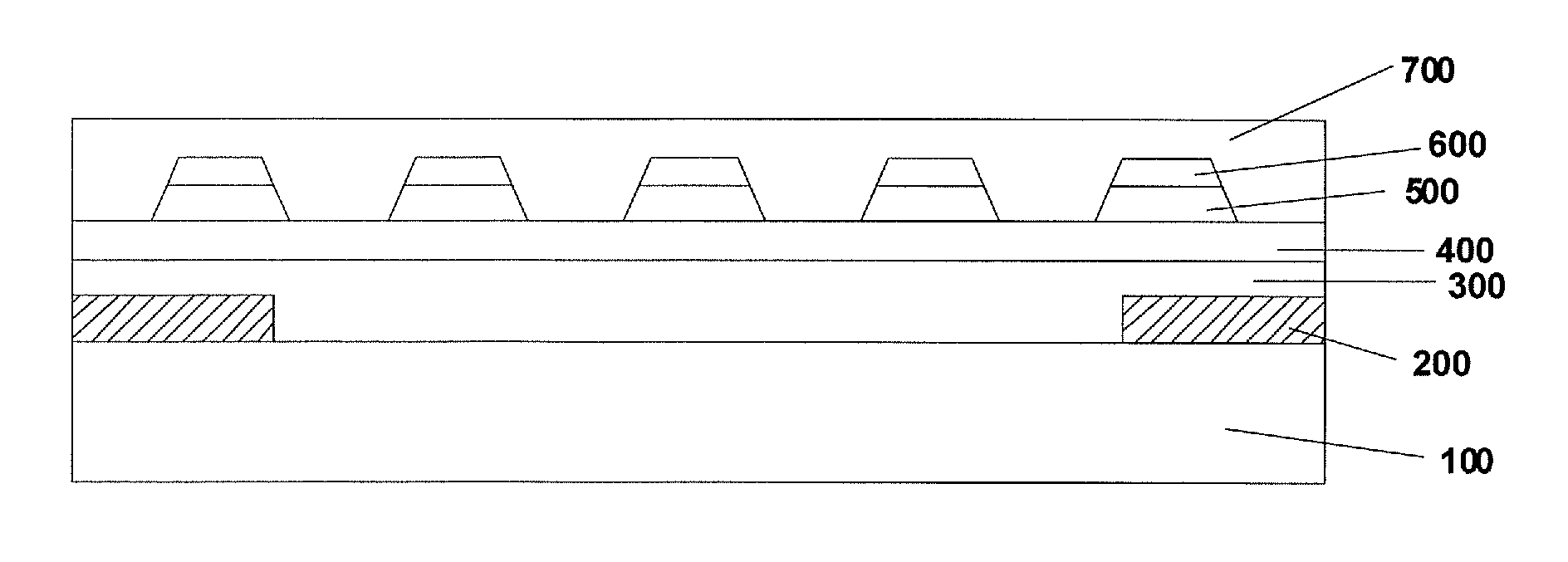
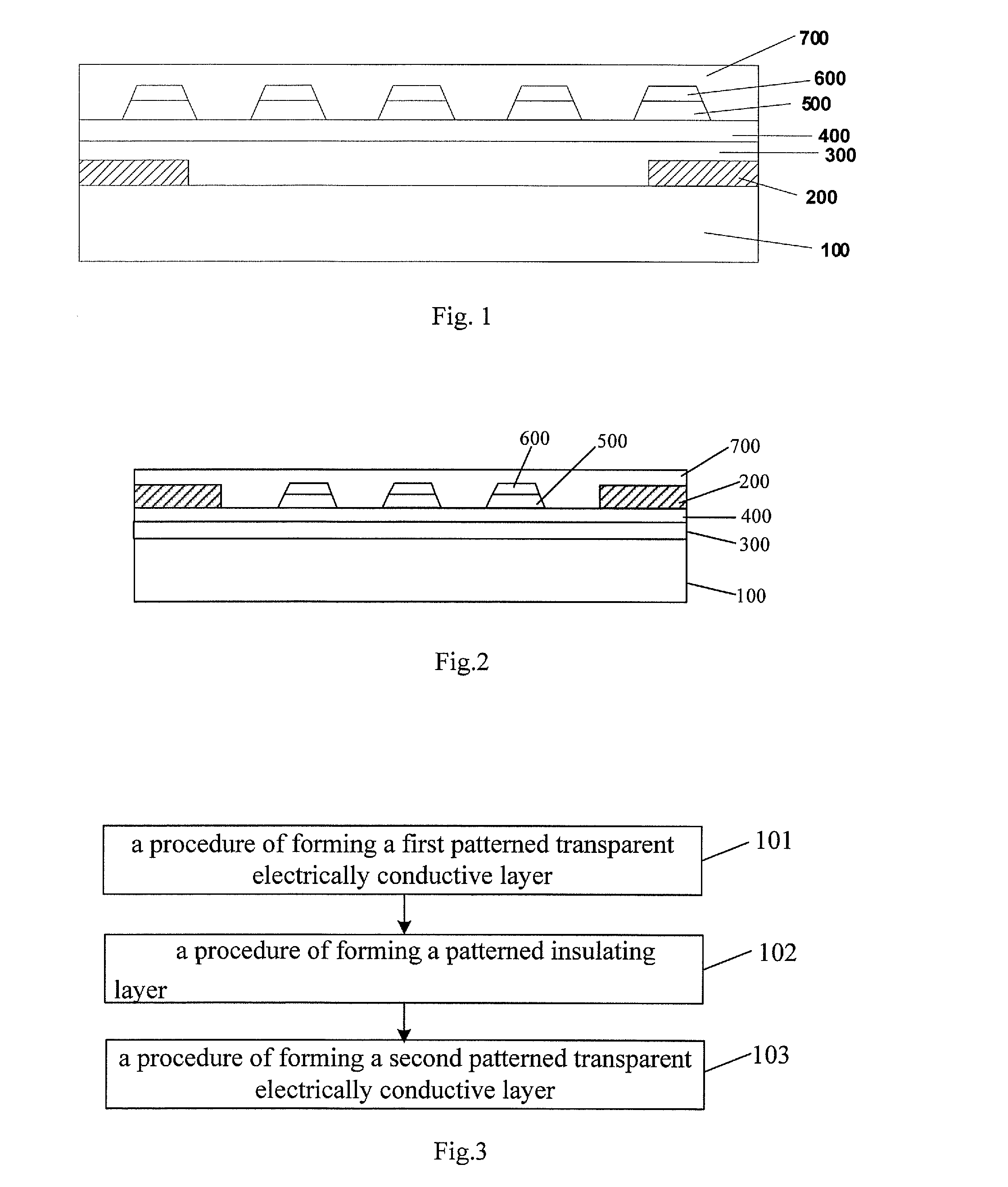
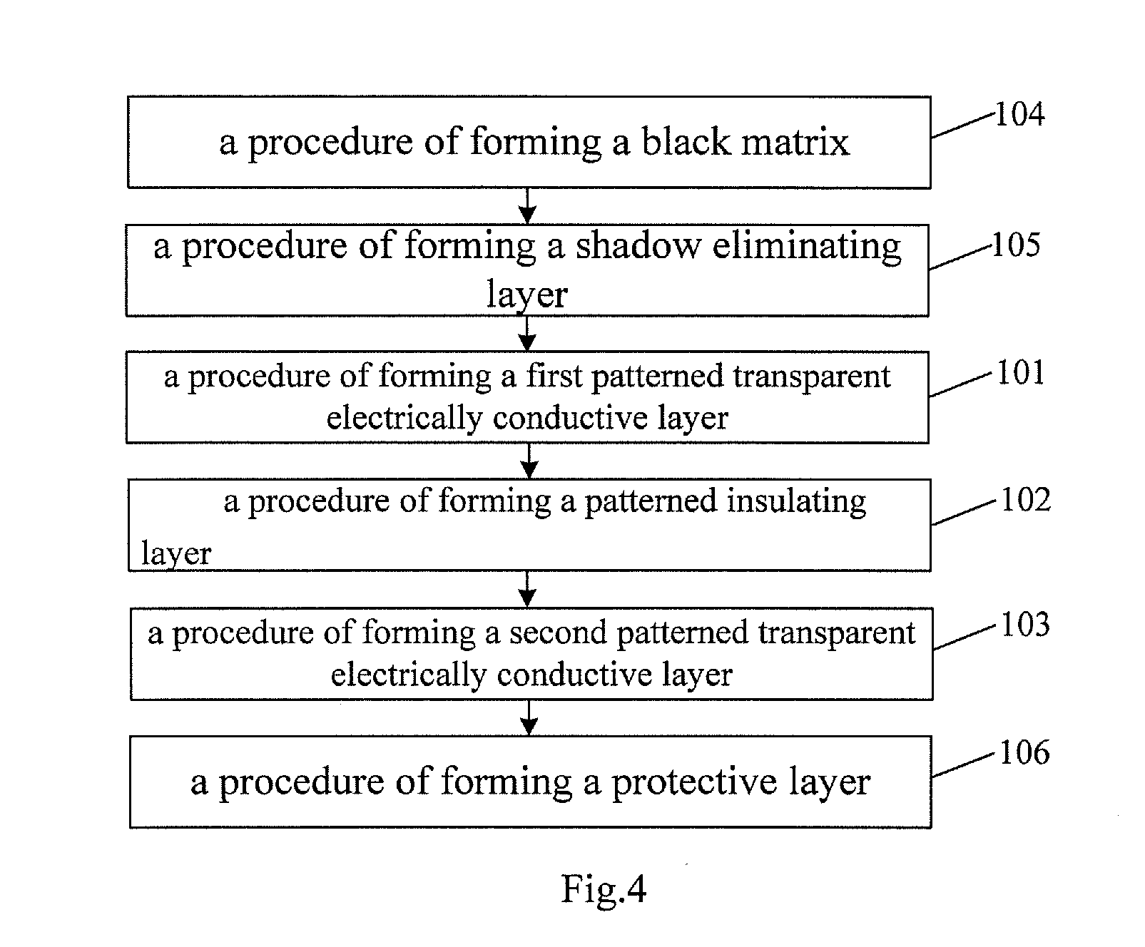
[0041]An embodiment of the present invention provides a touch screen, and the sectional view thereof is shown in FIG. 1. The touch screen may comprise: a transparent substrate 100, a first patterned transparent electrically conductive layer 400, a patterned insulating layer 500, and a second patterned transparent electrically conductive layer 600, wherein the first patterned transparent electrically conductive layer 400, the patterned insulating layer 500 and the second patterned transparent electrically conductive layer 600 may be successively formed above the transparent substrate 100; among the first patterned transparent electrically conductive layer 400 and the second patterned transp...


PUM


Abstract

The embodiments of the invention disclose a touch screen, a method for producing a touch screen, and a touch display device, which relate to a field of display. The touch screen does not need bridging, have high transmittance, and are simple in process, which can not only reduce the production cost but also achieve a high yield of mass production. The touch screen as provided in the embodiments of the invention comprises: a transparent substrate; a first patterned transparent eclectically conductive layer; a patterned insulating layer and a second patterned transparent eclectically conductive layer, which are formed above said transparent substrate successively, wherein among said first patterned transparent electrically conductive layer and said second patterned transparent electrically conductive layer, one is formed with a plurality of drive lines, and the other is formed with a plurality of induction lines; the pattern of said insulating layer is identical with that of said first patterned transparent electrically conductive layer, or identical with that of said second patterned transparent electrically conductive layer.

Description

FIELD OF THE INVENTION[0001]The present invention relates to the field of display technology, in particular relates to a touch screen, a method for producing the touch screen, and a touch display device.BACKGROUND OF THE INVENTION[0002]Touch display has been developed rapidly and has gradually been developed into a main-trend flat-panel display. At present, the touch display is mostly manufactured by laminating a touch screen having touch control function to a display panel. And the touch screen is often of capacitive sensing, when a finger (or other object) approaches or touches the touch screen, it would influence the capacitance between a drive line and an induction line which intersect each other around a touch point. The position of the touch point can be identified by detecting a change in the capacitance between the drive line and the induction line.[0003]With consumers' requirement for thinning of the touch display, technologists have developed many techniques to produce thi...

Claims


Application Information

Patent Timeline
IPC IPC(8): G06F3/044G06F3/041H05K3/02H05K3/46
CPCG06F3/044G06F3/041H05K3/467H05K3/027H05K2203/0502G06F2203/04103G06F2203/04104H05K2203/0361H05K3/4647G06F3/0445G06F3/0446H05K2201/0108H05K2201/0326H05K2201/10128
Inventor LIU, GUODONG
Owner BOE TECH GRP CO LTD
Learn More