Eureka AIR delivers breakthrough ideas for toughest innovation challenges, trusted by R&D personnel around the world.

Semiconductor light emitting element

Active Publication Date: 2016-03-24
STANLEY ELECTRIC CO LTD
View PDF1 Cites 5 Cited by
  • Summary
  • Abstract
  • Description
  • Claims
  • Application Information

AI Technical Summary

Benefits of technology

The technical effect of this patent is to prevent the lowering of luminous efficiency in semiconductor devices caused by the threading dislocation reaching the active layer. The pit function method is used to create a recess portion in the threading dislocation to prevent carriers from reaching it and reducing its quantum efficiency. Additionally, an electron blocking layer is used to prevent electrons from overflowing into the p-type semiconductor layer and improve luminous efficiency.

Problems solved by technology

When a semiconductor light emitting element is fabricated such that a nitride semiconductor layer is grown on a substrate made of a material different from the nitride semiconductor such as a sapphire substrate, crystal defects (misfit dislocations) occur at an interface between the substrate and the semiconductor layer due to their lattice mismatch.

Method used


Image

  • Semiconductor light emitting element
  • Semiconductor light emitting element
  • Semiconductor light emitting element

Examples


first embodiment

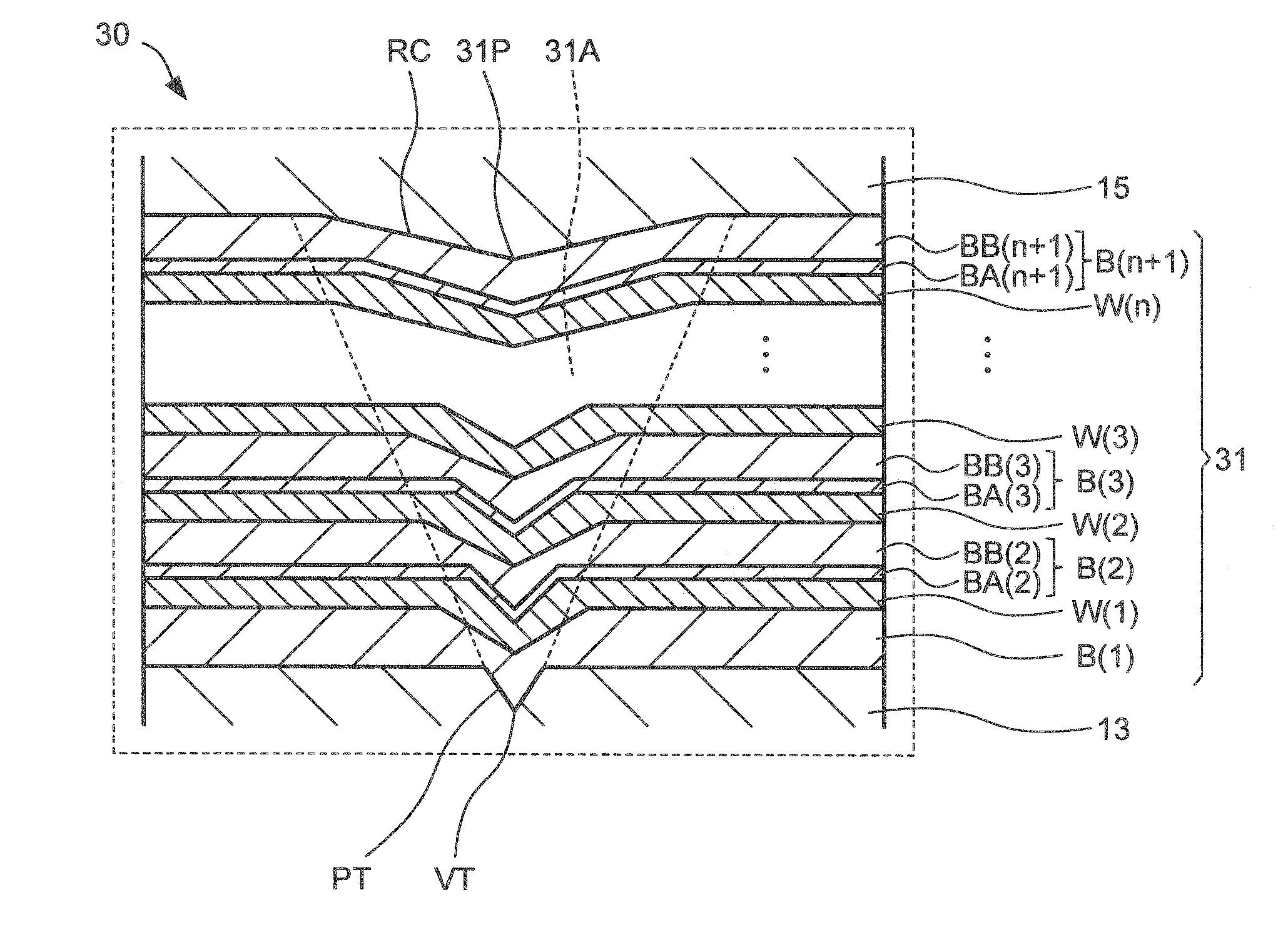
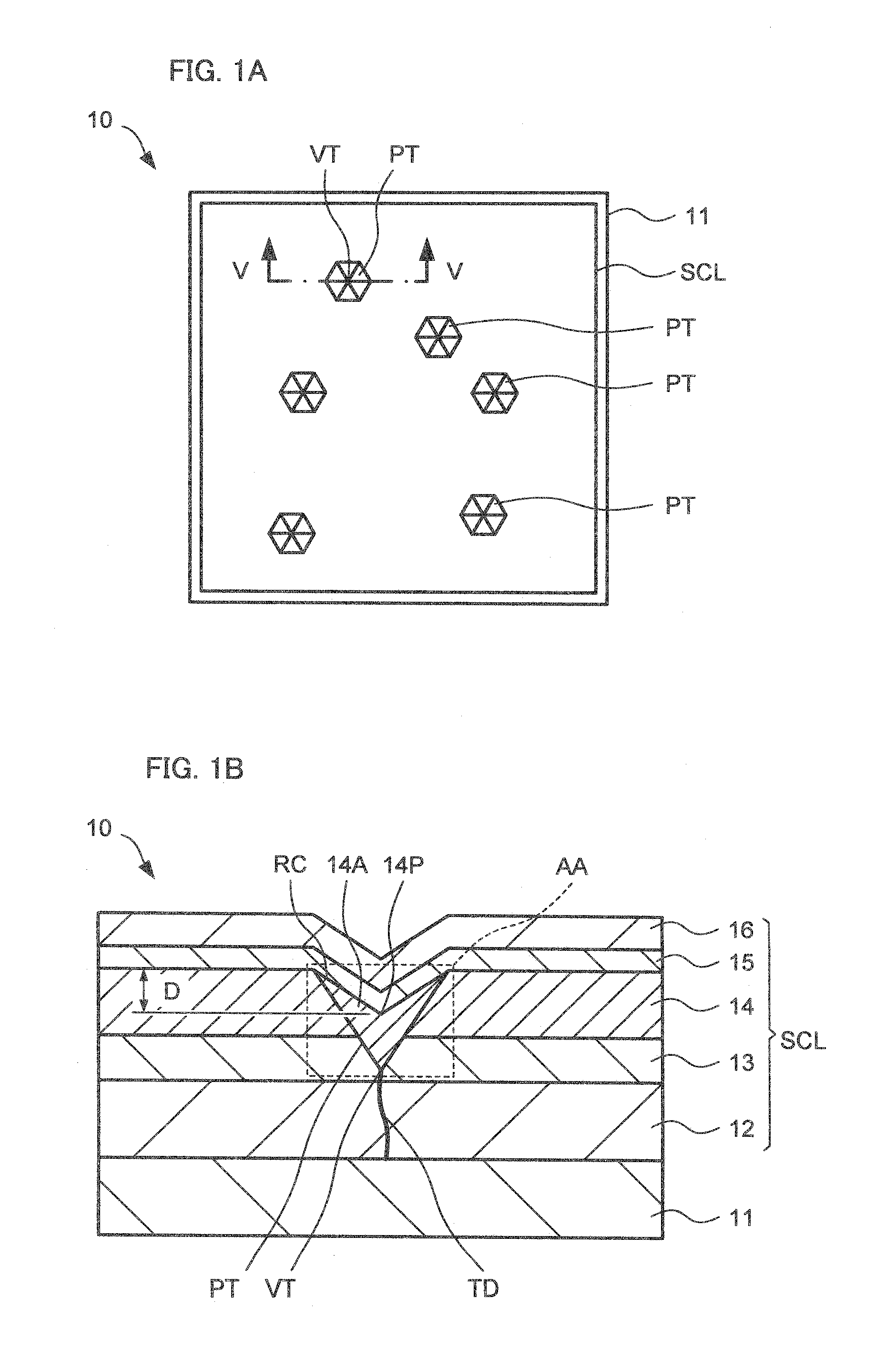
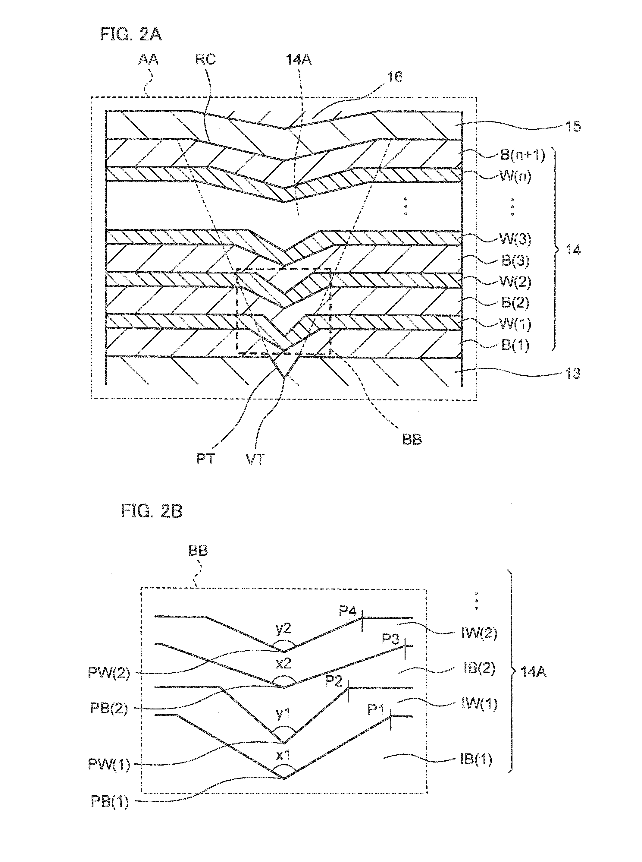
[0029]FIG. 1A shows a top view of a semiconductor light emitting element 10 (hereinafter simply referred to as the light emitting element or element) according to the first embodiment. FIG. 1B shows a cross-sectional view schematically partially illustrating a configuration of the semiconductor light emitting element 10. FIG. 1B shows a cross-section cut along a line V-V shown in FIG. 1A. The light emitting element 10 has a semiconductor structure layer SCL formed on a substrate 11. The semiconductor structure layer SCL has a threading dislocation TD which is caused by the lattice mismatch between the substrate 11 and the semiconductor structure layer SCL. The semiconductor structure layer SCL has a pyramidal pit PT due to the threading dislocation TD.

[0030]In the present embodiment, the semiconductor structure layer SCL is made from nitride-based semiconductors. Hereinafter a situation that the pit PT has a hexagonal pyramid-shaped form is described. Further, the present embodiment...


PUM


Abstract

A semiconductor light emitting element includes: a pit formation layer having a pyramidal pit caused by a threading dislocation generated in the first semiconductor layer; an active layer; and an electron blocking layer formed on the active layer to cover the recess portion. The active layer is formed on the pit formation layer and having an embedded portion formed so as to embed the pit and a recess portion formed on a surface of the embedded portion to correspond to the pit. The recess portion of the active layer has an apex formed at a position existing in a layered direction of the active layer within the active layer.

Description

BACKGROUND OF THE INVENTION[0001]1. Field of the Invention[0002]The present invention relates to a semiconductor light emitting element such as a light emitting diode (LED).[0003]2. Description of the Related Art[0004]The semiconductor light emitting element is fabricated typically by forming, on a growth substrate, an n-type semiconductor layer, a light emitting layer, and a p-type semiconductor layer, and then by forming an n-electrode and a p-electrode which apply a voltage to the n-type semiconductor layer and the p-type semiconductor layer. When the semiconductor light emitting element is fabricated to use a nitride-based semiconductor material, a sapphire substrate is used as a growth substrate, for example.[0005]Japanese Patent Application Kokai No. 2013-41930 discloses a nitride semiconductor light emitting element which comprises an n-type nitride semiconductor layer, a V-pit generation layer, an intermediate layer, a multiple quantum well light emitting layer, and a p-type...

Claims


Application Information

Patent Timeline
IPC IPC(8): H01L33/06H01L33/20H01L33/32
CPCH01L33/06H01L33/32H01L33/20H01L21/02458H01L21/02505H01L21/02513H01L21/0254H01L21/0259H01L33/02H01L33/025
Inventor YAMANE, TAKAYOSHILIANG, JI-HAO
Owner STANLEY ELECTRIC CO LTD
Why Eureka
Eureka Blog
Learn More