
Microlens array substrate, electrooptical device including microlens array substrate, projection type display apparatus, and manufacturing method of microlens array substrate

a microlens array and electrooptical device technology, applied in the field of microlens array substrates, can solve the problems of microlens array substrate warping or deformation due to thermal expansion, microlens array substrate quality decline, display quality reduction,

Active Publication Date: 2016-04-07
SEIKO EPSON CORP
View PDF11 Cites 9 Cited by
  • Summary
  • Abstract
  • Description
  • Claims
  • Application Information

AI Technical Summary

Benefits of technology

The patent describes a microlens array substrate used in display devices. By using a light transmitting layer with a smaller refractive index and coefficient of thermal expansion than the lens layers, the incident light is refracted to the oblique side, resulting in a significant curve of the light. This allows for a smaller total film thickness of the substrate, improved transmittance without lengthening the distance between the lenses, and prevents warping or deformation of the substrate. As a result, the display quality is improved.

Problems solved by technology

However, when a thickness of the microlens array substrate (microlens) increases, the microlens array substrate may be warped or deformed due to thermal expansion.
As a result, unevenness or black floating may be generated and display quality may be decreased.
In addition, processing variation in the microlens (first lens and second lens) negatively affects the quality of the microlens and the image quality is deteriorated.

Method used


Image

  • Microlens array substrate, electrooptical device including microlens array substrate, projection type display apparatus, and manufacturing method of microlens array substrate
  • Microlens array substrate, electrooptical device including microlens array substrate, projection type display apparatus, and manufacturing method of microlens array substrate
  • Microlens array substrate, electrooptical device including microlens array substrate, projection type display apparatus, and manufacturing method of microlens array substrate

Examples


first embodiment

[0047]In the embodiment, an active matrix type liquid crystal device including a thin film transistor (TFT) as a switching element of a pixel will be described as an example of an electrooptical device including a microlens array substrate. This liquid crystal device, for example, can be suitably used as an optical modulation unit (liquid crystal light bulb) of a projection type display apparatus (liquid crystal projector) which will be described later.

Configuration of Microlens Array Substrate

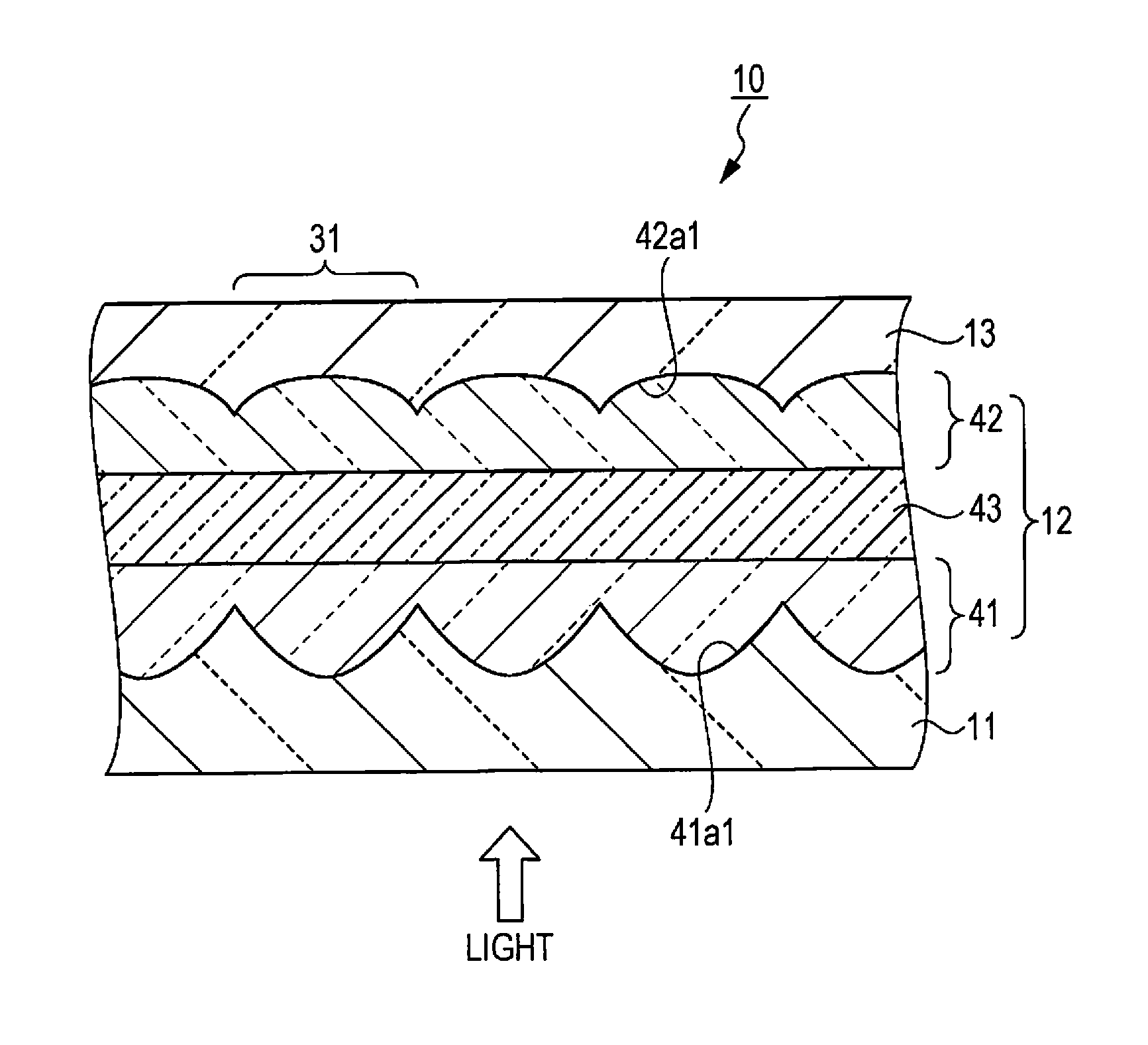
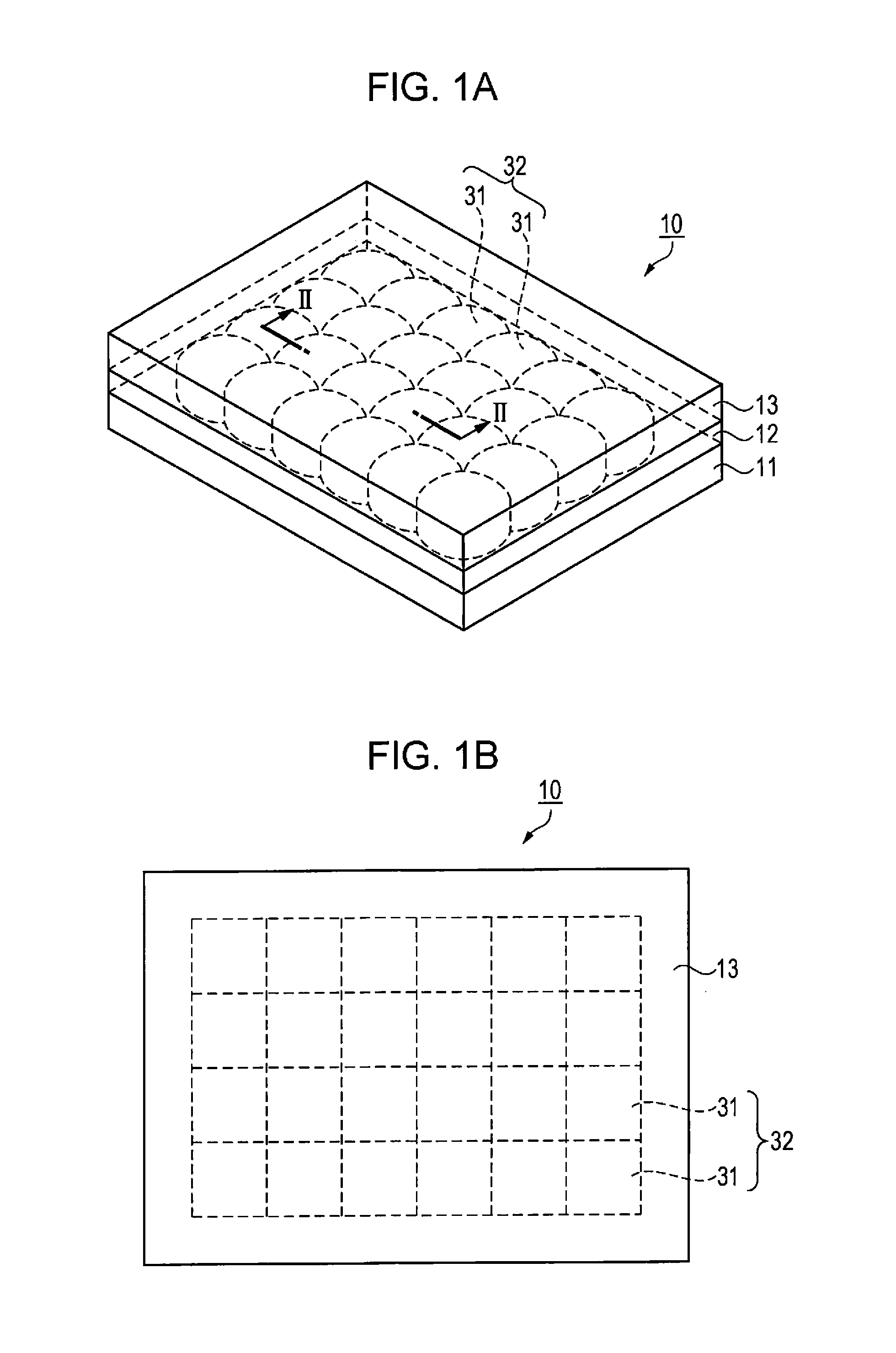
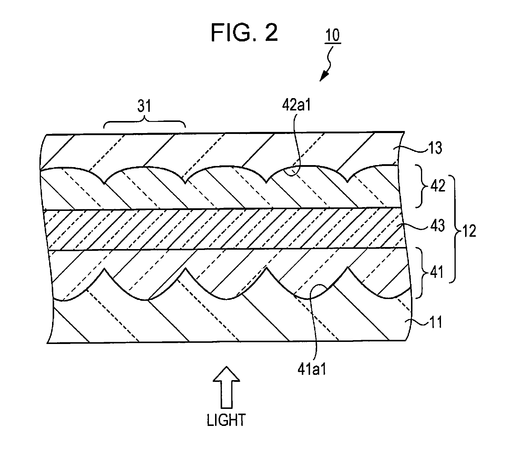
[0048]FIGS. 1A and 1B are schematic views showing a configuration of the microlens array substrate. FIG. 1A is a schematic perspective view showing the configuration of the microlens array substrate. FIG. 1B is a schematic plan view of the microlens array substrate of FIG. 1A in a top view. FIG. 2 is a schematic sectional view of the microlens array substrate shown in FIG. 1A taken along line II-II. Hereinafter, the configuration of the microlens array substrate will be described with referenc...

second embodiment

Configuration of Microlens Array Substrate

[0109]FIG. 9 is a schematic sectional view showing a configuration of a microlens array substrate of a second embodiment. Hereinafter, the configuration of the microlens array substrate will be described with reference to FIG. 9.

[0110]A microlens array substrate 20 of the second embodiment is different from the microlens array substrate 10 of the first embodiment in that the first lens 41a and the second lens 42a are laminated by a plurality of different refractive index layers, and the other parts thereof are substantially the same. Accordingly, in the second embodiment, the parts different from that of the first embodiment will be described in detail and the description of the other overlapping parts will be suitably omitted.

[0111]As shown in FIG. 9, the microlens array substrate 20 of the second embodiment includes the light transmitting substrate 11, a first lens layer 141 including a plurality of microlenses 131, the light transmitting ...

modification example 1

[0134]As described above, there is no limitation of using the liquid crystal device 100 as the electrooptical device, and an organic EL device, a plasma display, an electronic paper (EPD), or an imaging device such as a CCD or a CMOS may be used.


PUM

PropertyMeasurementUnit
refractive indexaaaaaaaaaa
thicknessaaaaaaaaaa

Abstract

A microlens array substrate includes: a light transmitting substrate in which a first lens surface formed of a concave surface is formed on a substrate surface on one side; a first lens layer which covers the substrate surface on one side and has a refractive index which is different from that of the light transmitting substrate; a light transmitting layer which covers the first lens layer on the opposite side to the light transmitting substrate; and a second lens layer which covers the light transmitting layer on the opposite side to the light transmitting substrate and in which a second lens surface formed of a convex surface is formed on the opposite side to the light transmitting substrate, in which the light transmitting layer has smaller refractive index and coefficient of thermal expansion than those of the first lens layer and the second lens layer.

Description

BACKGROUND[0001]1. Technical Field[0002]The present invention relates to a microlens array substrate, an electrooptical device including a microlens array substrate, a projection type display apparatus, and a manufacturing method of a microlens array substrate.[0003]2. Related Art[0004]As the microlens array substrate, a microlens array substrate in which a plurality of microlenses are arranged on a substrate has been known. The microlens array substrate including a plurality of microlenses, is, for example, disposed between a light source and a liquid crystal light bulb in a liquid crystal projector, and has been used for various purposes such as, for preventing loss of light quantity or increasing an amount of incident light.[0005]JP-A-2014-89230, for example, discloses a microlens array (substrate) including a plurality of first lenses, and a plurality of second lenses each of which is disposed to face each of the first lenses, in order to further increase usage efficiency of lig...

Claims


Application Information

Patent Timeline
Patent Type & Authority Applications(United States)
IPC IPC(8): G02B3/00G02F1/1362G02F1/1335
CPCG02B3/0056G02B3/0068G02F1/1362G02F1/133526G02B3/0012
Inventor WAKABAYASHI, JUNICHI
Owner SEIKO EPSON CORP
Learn More