

Quasi-crystal organic light-emitting display panel and method for simulating optical efficiency of the same
- Summary
- Abstract
- Description
- Claims
- Application Information
AI Technical Summary
Benefits of technology
Problems solved by technology
Method used
Image

Examples
Embodiment Construction
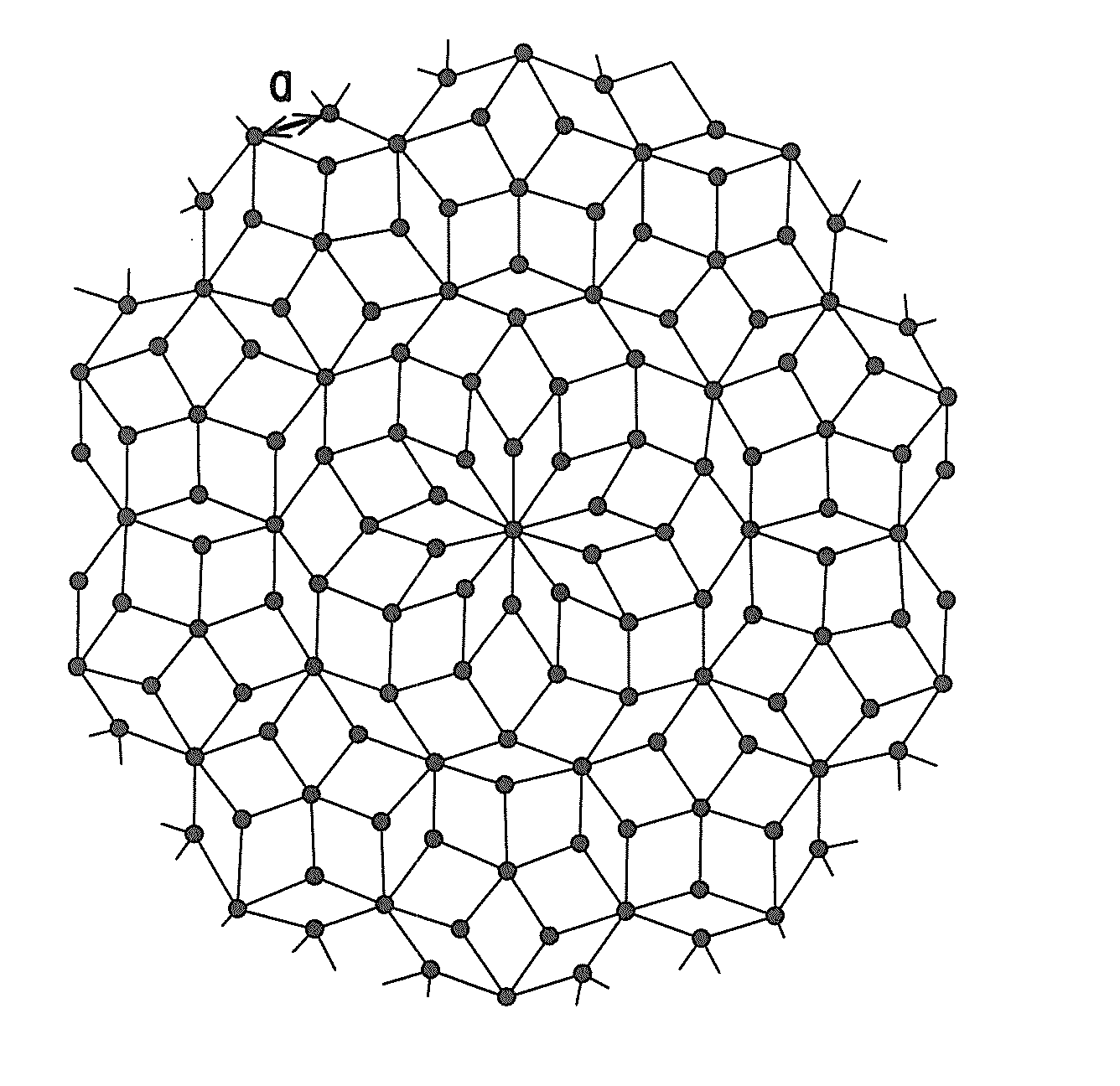
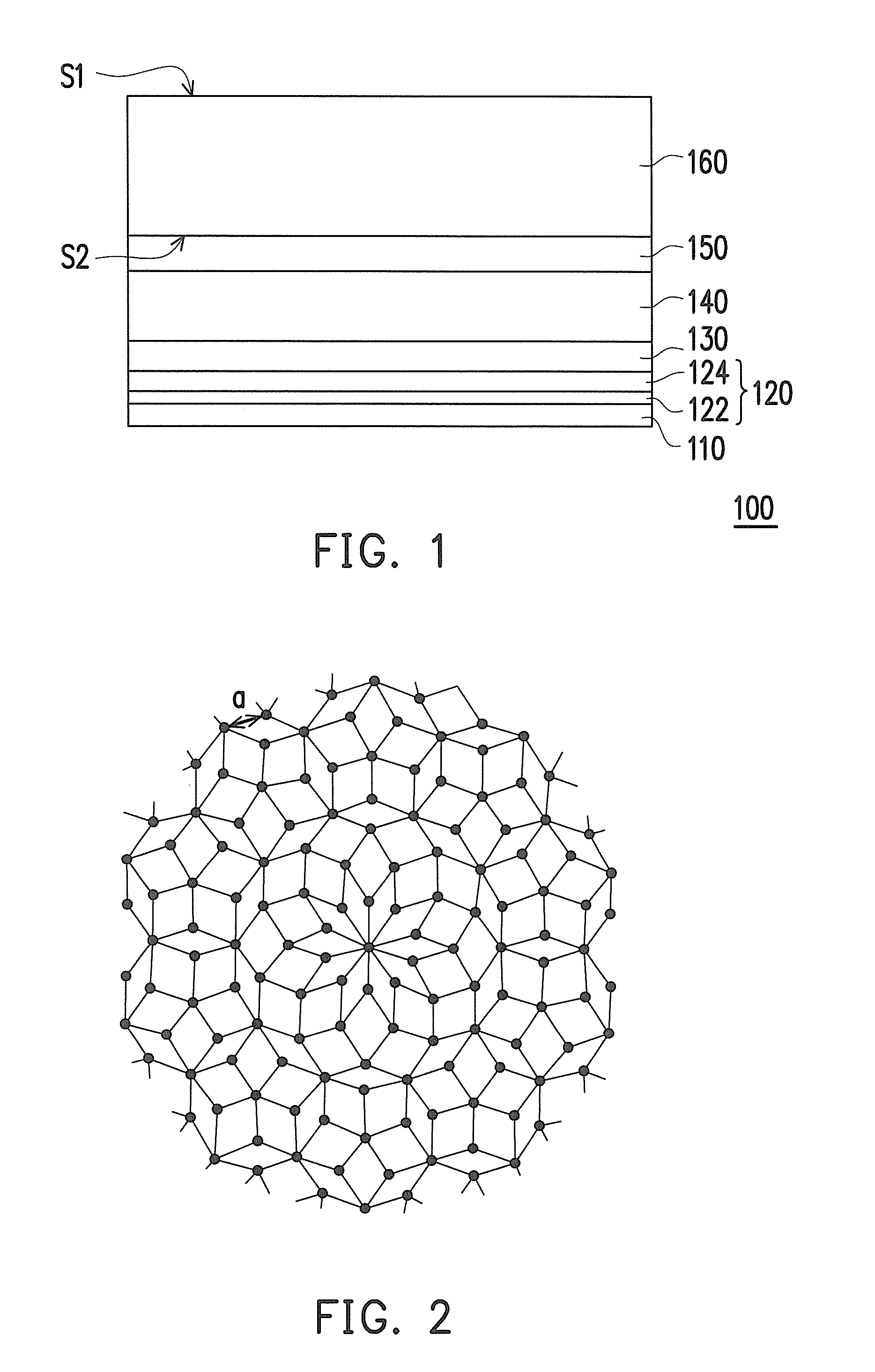
[0018]FIG. 1 is a cross-sectional view of an organic light-emitting display panel according to an embodiment of the invention. FIG. 2 is a top view of a 10-fold quasi-crystal layer in FIG. 1. Referring to FIG. 1, the quasi-crystal organic light-emitting display panel 100 includes a first electrode layer 110, an organic light-emitting layer 120, a second electrode layer 130, a buffer layer 140, a 10-fold quasi-crystal layer 150 and a package cover 160. The organic light-emitting layer 120 is located on the first electrode layer 110. The second electrode layer 130 is located on the organic light-emitting layer 120. The buffer layer 140 is located on the second electrode layer 130. The 10-fold quasi-crystal layer 150 is located on the buffer layer 140. The package cover 160 is located on the 10-fold quasi-crystal layer 150.
[0019]As shown in FIG. 1, the package cover 160 has an outer surface S1 and an inner surface S2 opposite to the outer surface S1. The 10-fold quasi-crystal layer 150...
PUM
 Abstract
Description
Claims
Application Information