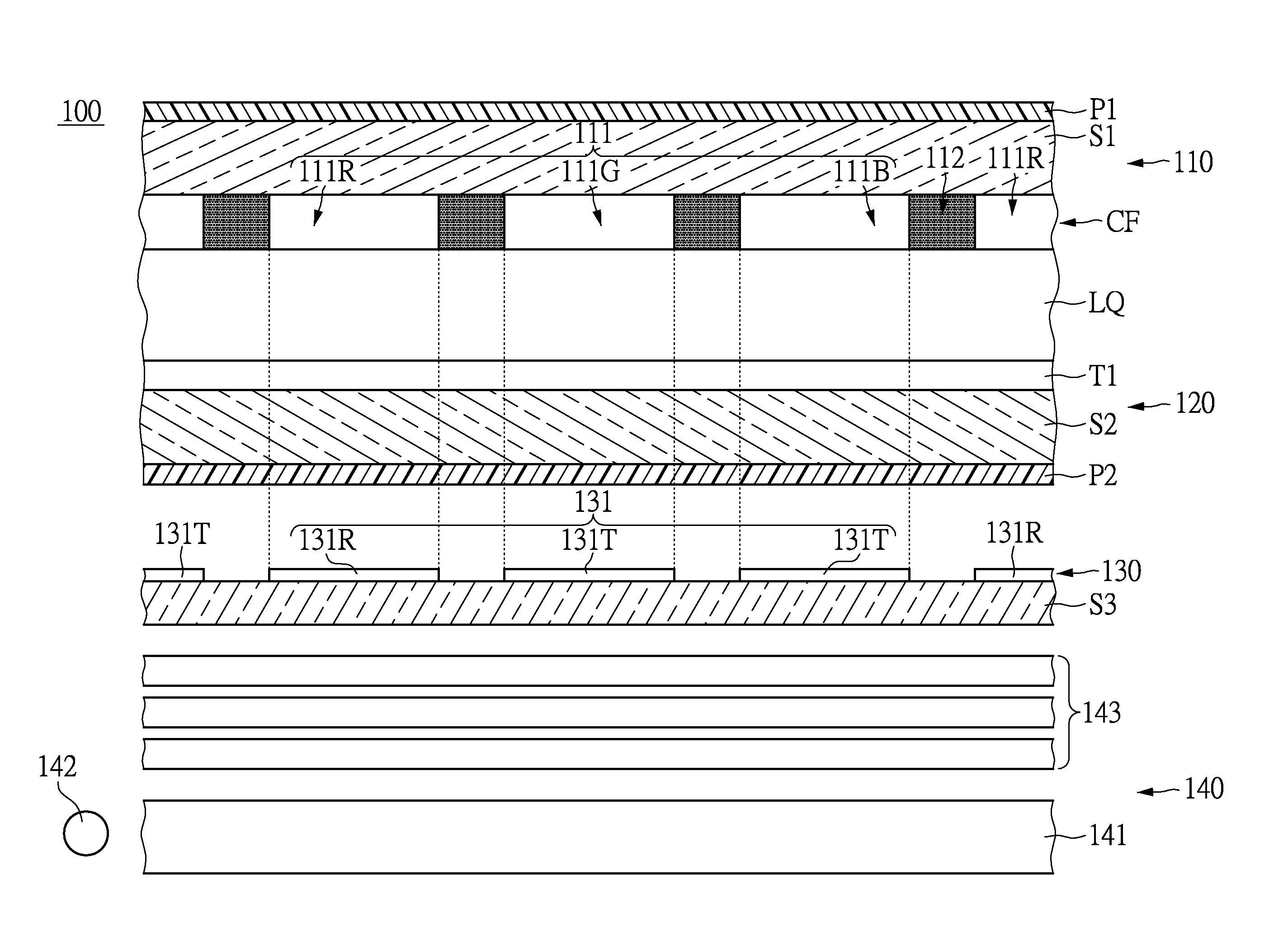
Display device

a display frame and liquid crystal display technology, applied in the field of display frames, can solve the problems of affecting the appearance, the relative difficulty of achieving pure color and the wide color gamut of the display frame of the liquid crystal display, and achieve the effect of wide color gamut and pure color

Active Publication Date: 2016-04-28
INNOLUX CORP
View PDF12 Cites 21 Cited by
  • Summary
  • Abstract
  • Description
  • Claims
  • Application Information

AI Technical Summary

Benefits of technology

[0007]An embodiment of the instant disclosure provides a display device which can achieve pure color and wide color gamut.

Problems solved by technology

Therefore, it is relatively hard to achieve pure color and wide color gamut in the display frame of the liquid crystal display.

Method used


Image

  • Display device
  • Display device
  • Display device

Examples


second embodiment

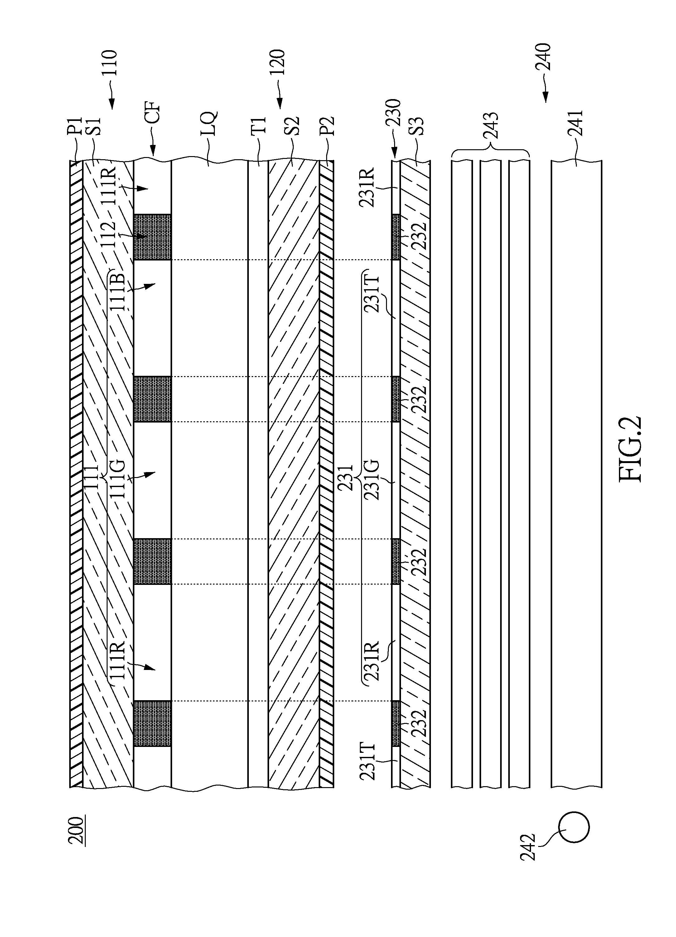
[0034]FIG. 2 is a schematic structural view of a display device in accordance with the instant disclosure. On the basis of the above mentioned display device, there is provided another quantum dot pattern layer 230 and backlight module 240. Most of the implementation details refer to the foregoing description, and the common features are not described again.

[0035]Please refer to FIG. 2, the quantum dot pattern layer 230 is located between the second substrate S2 and the backlight module 240. In practice, the display device further includes a third substrate S3 disposed between the second substrate S2 and the backlight module 240. The quantum dot pattern layer 230 is disposed on the third substrate S3. The quantum dot pattern layer 230 includes at least one quantum dot pattern 231 corresponding to one of the filter patterns 111, and the color of the quantum dot pattern 231 is identical to the color of the filter pattern 111. In this embodiment, the quantum dot pattern layer 230 consi...

third embodiment

[0040]FIG. 3 is a schematic structural view of a display device in accordance with the instant disclosure. On the basis of above mentioned display device, there is provided another quantum dot pattern layer 330. Most of the implementation details refer to the foregoing description, and the common features are not described again.

[0041]In this embodiment, the display device 300 does not include the backlight module, and the quantum dot pattern layer 330 disposing between the first substrate S1 and the second substrate S2 can be used as a display medium layer. In this embodiment, the quantum dot pattern layer 330 is an electroluminescent quantum dot pattern layer so that the active element array layer T1 with a patterned electrode layer can control the brightness of the pixel of the quantum dot pattern layer 330 to change the grayscale value of pixel. The active element array layer T1 with a patterned electrode layer can be disposed on, but is not limited to, the second substrate S2. ...


PUM

PropertyMeasurementUnit
coloraaaaaaaaaa
widthaaaaaaaaaa
wavelengthaaaaaaaaaa

Abstract

A display panel includes a first substrate, a second substrate, a display medium layer, a color filter layer, a third substrate, a backlight module, and a quantum dot pattern layer. The display medium layer and the color filter layer are disposed between the first and second substrates. The color filter layer includes a first color filter pattern. The backlight module is disposed on one side of the second substrate. The second and the third substrate are disposed between the backlight module and the display medium layer, and between the backlight module and the second substrate, respectively. The quantum dot pattern layer is disposed on the third substrate and between the third substrate and the second substrate, and includes at least one first quantum dot pattern corresponding to first color filter pattern. The first quantum dot pattern's color is equal to the first color filter pattern's color.

Description

BACKGROUND[0001]1. Field of the Invention[0002]The instant disclosure relates to a display device, in particular, relates to a display device having a quantum dot pattern layer.[0003]2. Description of Related Art[0004]In general, the liquid crystal display includes an active element array substrate, color filter, polarizer films and backlight module. The active element array substrate is formed by disposing thin film transistors that control voltage of sub-pixels, so as to adjust the angle of the deflection of liquid crystal. Then, the gray scale data of sub-pixels can be adjusted. Through the color filter and the grey scale data of sub-pixels, the sub-pixels emitting red, blue and green light can produce an image.[0005]At present, most backlights of liquid crystal displays are blue light emitting diode chips with yellow phosphor (such as YAG or TAG) or blue light emitting diode chips accompanied with green phosphor and red phosphor.[0006]However, the peak of excitation spectrum of ...

Claims


Application Information

Patent Timeline
Patent Type & Authority Applications(United States)
IPC IPC(8): G02F1/1335F21V8/00
CPCG02F1/133617G02F1/133514G02F2001/133614G02B6/0073G02B6/0035G02F1/133528G02B6/005G02F2202/36G02F1/133614
Inventor FAN, KUO-JUNGMAO, LI-WEI
Owner INNOLUX CORP
Why Eureka
Try Eureka