

Semiconductor device
a semiconductor device and semiconductor technology, applied in the field of semiconductor devices, can solve the problems of reducing the size of the semiconductor device, affecting the performance of the device, and affecting the performance of the device, and achieve the effect of easy manufacturing of the devi
- Summary
- Abstract
- Description
- Claims
- Application Information
AI Technical Summary
Benefits of technology
Problems solved by technology
Method used
Image

Examples
first embodiment
[0045]The present embodiment will be described in connection with an example of a semiconductor device that obtains a ground state of an Ising model. In the present embodiment, factorization is described as an example of a problem to be solved. Specifically, a problem in which a 4-bit number is factorized into two 2-bit values is converted into a problem for obtaining a ground state of an Ising model, and the problem is solved by a semiconductor device.
[0046]<Conversion of Problem that is Desired to be Solved into Ising Model)
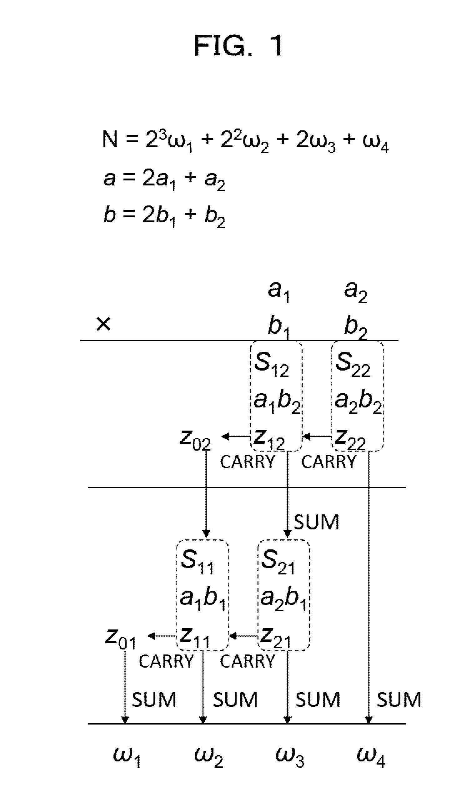
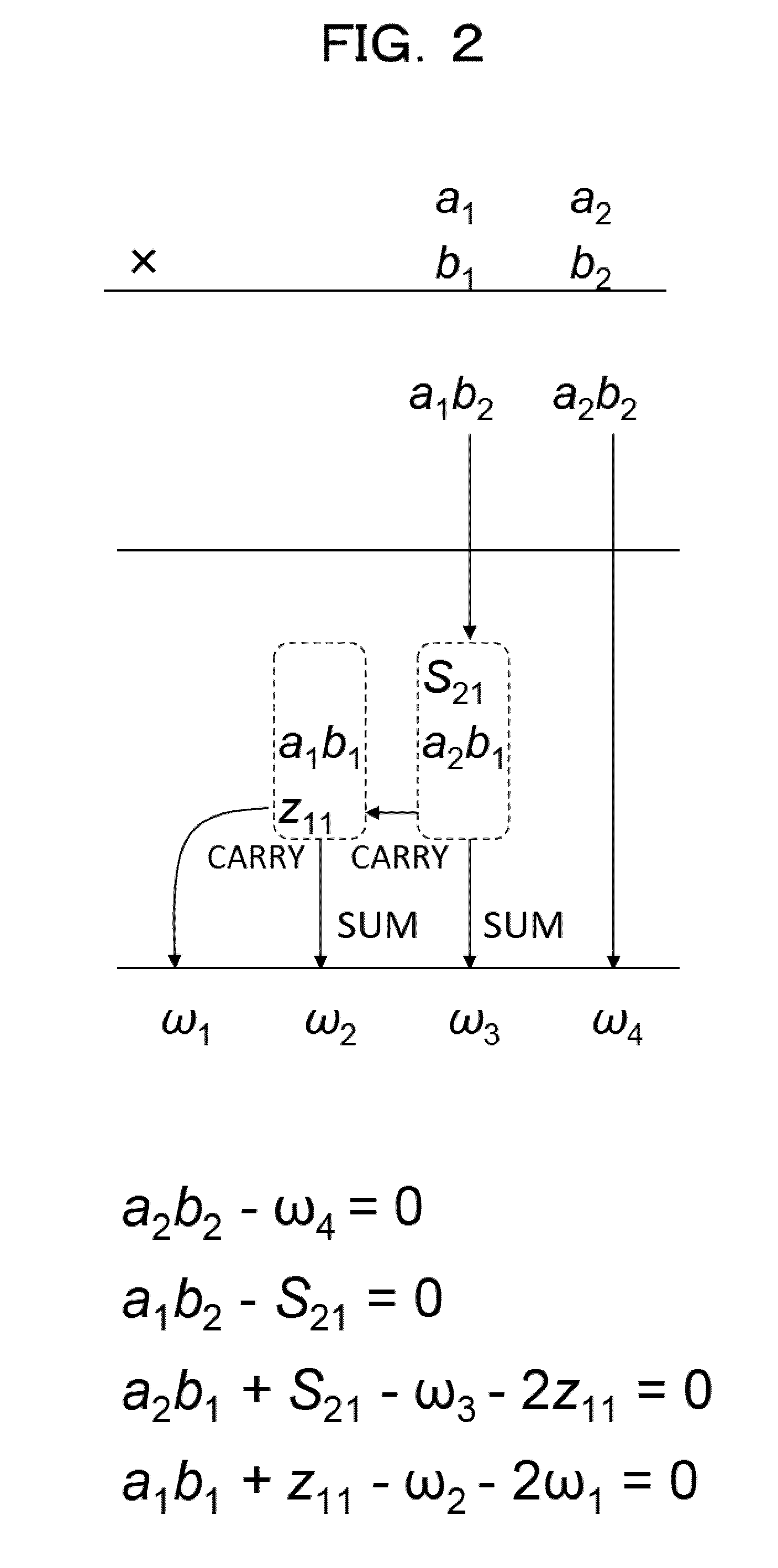
[0047]Obtaining the ground state of the Ising model is an optimization problem that obtains an arrangement of spins minimizing the energy function of the Ising model. Thus, first, factorization is formulated as an optimization problem. When a number to be factorized is N, and factors of N are a and b, factorization can be performed by obtaining a and b satisfying the following Formula (1):
[Expression 1]
(N−ab)2=0 (1)
[0048]Then, Formula (1) is expressed by a Ham...
second embodiment
Embodiment by Power Voltage Control of Memory Cell
[0099]FIG. 10 is a configuration diagram of a semiconductor device according to a second embodiment. A semiconductor device 1000 according to the present embodiment differs from the semiconductor device 300 according to the first embodiment in that power voltage of the memory cell is controlled such that the memory cell is stochastically inverted. The remaining points are the same as in the first embodiment, and thus a duplicated description is omitted.
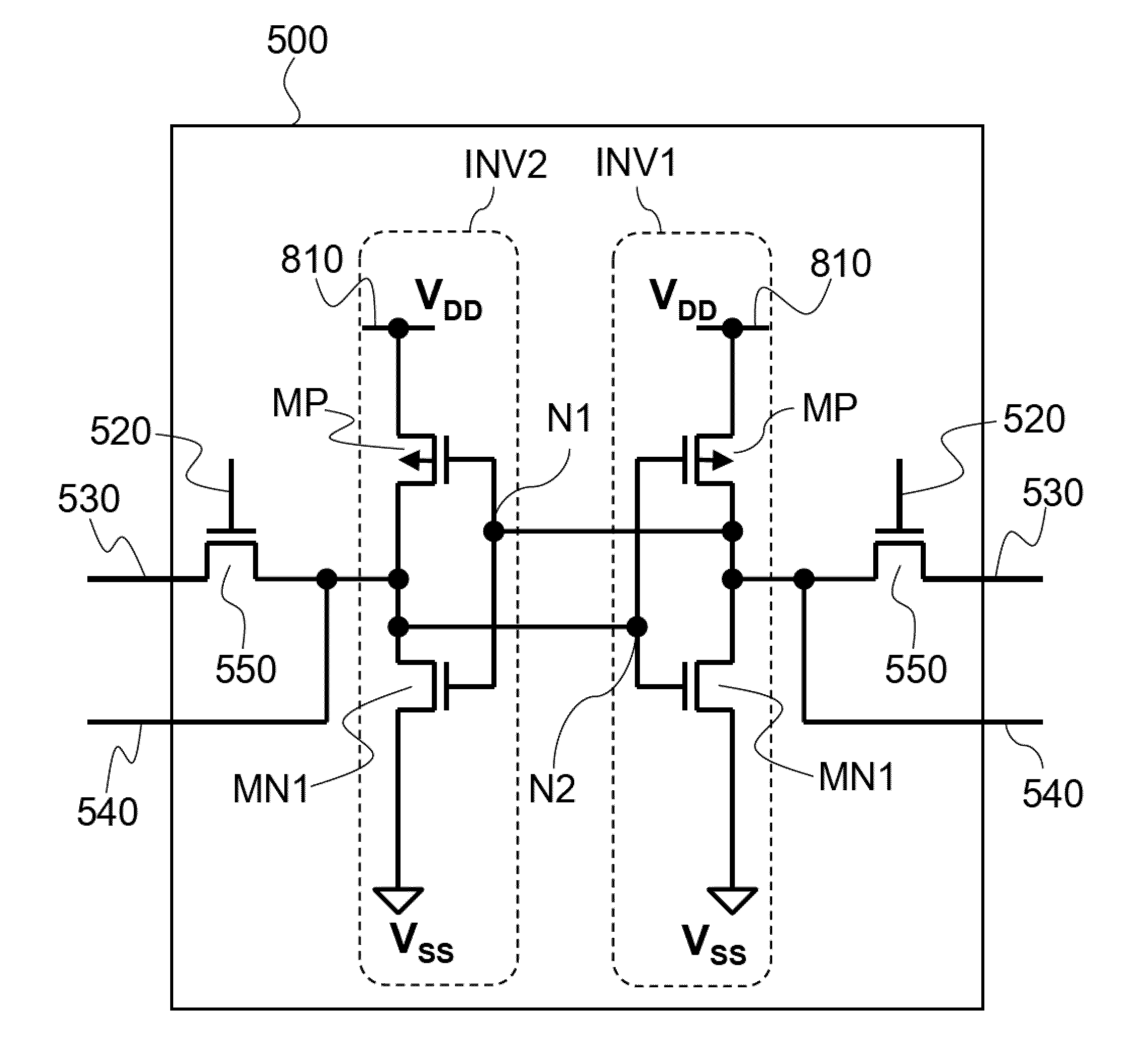
[0100]In the semiconductor device 1000, a memory cell array 310 is configured with the same memory cells 500 as in the first embodiment as illustrated in FIG. 8. CMOS inverters INV1 and INV2 are configured with a p-channel MOS transistor MP and an n-channel MOS transistor MN1. It is possible to control the power voltage of the memory cell 500 by controlling a voltage (VDD) supplied to a power line 810 of the memory cell 500. Commonly, a voltage of about 1 V is used as power voltage of ...
third embodiment
Embodiment by Trip Point Control of Memory Cell
[0102]FIG. 11 is a configuration example of a semiconductor device according to a third embodiment. A semiconductor device 1100 according to the present embodiment differs from the semiconductor device 300 according to the first embodiment and the semiconductor device 1000 according to the second embodiment in that a trip point (a voltage change point for causing the storage content to transition from 0 to 1 or from 1 to 0) of the memory cell is controlled in order to stochastically invert the memory cell. The remaining points are the same as in the first embodiment and the second embodiment, and thus a duplicated description is omitted.
[0103]In the semiconductor device 1100, a memory cell array 1120 is configured with memory cells 900 illustrated in FIG. 9. Compared to the memory cells 500 according to the first embodiment and the second embodiment, an n-channel MOS transistor MN2 that controls the trip point of the memory cell and a t...
PUM
 Abstract
Description
Claims
Application Information