Manufacturing flexible organic electronic devices

a flexible, organic technology, applied in sustainable manufacturing/processing, identification means, instruments, etc., can solve the problems of longer tac time and more complex material structure, and achieve the effect of sufficient tension

Inactive Publication Date: 2016-05-12
UNIVERSAL DISPLAY
View PDF6 Cites 2 Cited by
  • Summary
  • Abstract
  • Description
  • Claims
  • Application Information

AI Technical Summary

Problems solved by technology

Organic-inorganic stacks are particularly good at covering particulate defects on the OLED surface (however, at the expense of a longer TAC time and more complex material structure).

Method used


Image

  • Manufacturing flexible organic electronic devices
  • Manufacturing flexible organic electronic devices
  • Manufacturing flexible organic electronic devices

Examples


Embodiment Construction

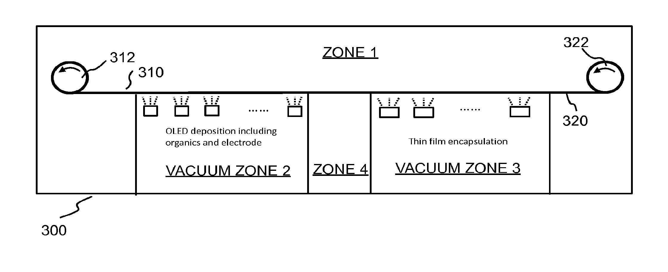
[0056]The methods, devices and systems hereof can be used in connection with organic electronic devices generally. A number of representative embodiments thereof are discussed in connection with representative embodiments of flexible OLEDs formed in continuous, roll-to-roll processes.

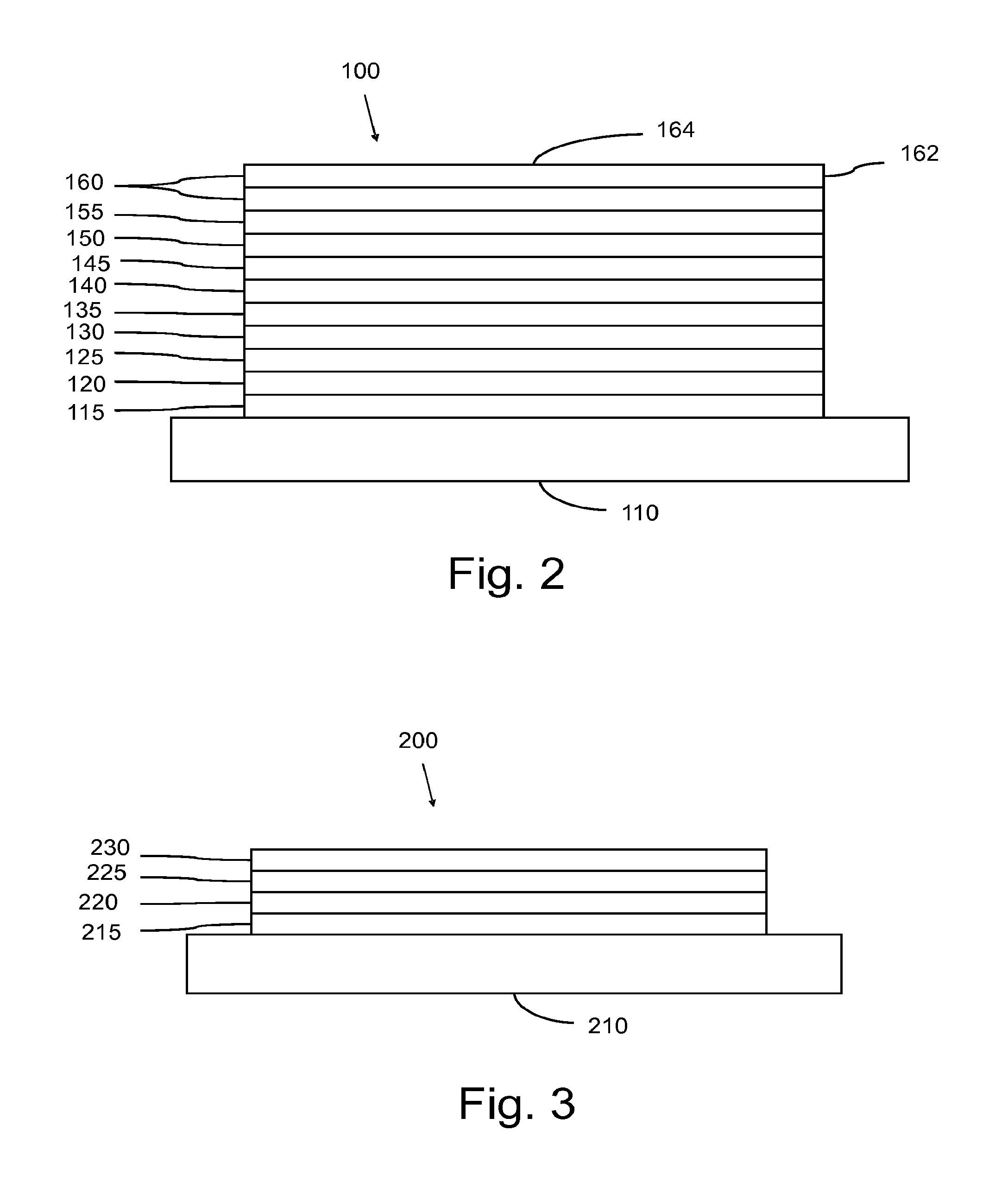
[0057]Generally, an OLED comprises at least one organic layer disposed between and electrically connected to an anode and a cathode. When a current is applied, the anode injects holes and the cathode injects electrons into the organic layer(s). The injected holes and electrons each migrate toward the oppositely charged electrode. When an electron and hole localize on the same molecule, an “exciton,” which is a localized electron-hole pair having an excited energy state, is formed. Light is emitted when the exciton relaxes via a photoemissive mechanism. In some cases, the exciton may be localized on an excimer or an exciplex. Non-radiative mechanisms, such as thermal relaxation, may also occur, but are g...


PUM

PropertyMeasurementUnit
timeaaaaaaaaaa
humidityaaaaaaaaaa
pressureaaaaaaaaaa

Abstract

A method of forming microelectronic systems on a flexible substrate includes depositing (typically sequentially) on a first side of the flexible substrate at least one organic thin film layer, at least one electrode and at least one thin film encapsulation layer over the at least one organic thin film layer and the at least one electrode, wherein depositing the at least one organic thin film layer, depositing the at least one electrode and depositing the at least one thin film encapsulation layer each occur under vacuum and wherein no physical contact of the at least one organic thin film layer or the at least one electrode with another solid material occurs prior to depositing the at least one thin film encapsulation layer.

Description

[0001]The claimed invention was made by, on behalf of, and / or in connection with one or more of the following parties to a joint university corporation research agreement: Regents of the University of Michigan, Princeton University, The University of Southern California, and the Universal Display Corporation. The agreement was in effect on and before the date the claimed invention was made, and the claimed invention was made as a result of activities undertaken within the scope of the agreement.FIELD[0002]In a number of embodiments, devices, systems and methods hereof relate to organic electronic devices including, for example, organic light-emitting diode devices and manufacture thereof.BACKGROUND[0003]The following information is provided to assist the reader in understanding technologies disclosed below and the environment in which such technologies may typically be used. The terms used herein are not intended to be limited to any particular narrow interpretation unless clearly s...

Claims


Application Information

Patent Timeline
Patent Type & Authority Applications(United States)
IPC IPC(8): H01L51/00H01L51/52
CPCH01L51/001H01L51/0021H01L2251/56H01L51/0097H01L2251/5338H01L51/5253H10K71/10H10K71/00C23C14/562C23C14/568Y02E10/549Y02P70/50H10K71/164H10K85/342H10K50/00H10K50/80H10K50/10H10K77/111H10K50/844H10K71/60H10K2102/311
Inventor MA, RUIQINGSILVERNAIL, JEFFREYMANDLIK, PRASHANTBROWN, JULIA J.FELTS, JOHN
Owner UNIVERSAL DISPLAY
Why Eureka
Try Eureka