Substrate-less electronic component and the method to fabricate thereof

a technology of electronic components and substrates, applied in the direction of magnets, inductances, magnetic bodies, etc., can solve the problem that the increase in the bandwidth used in communication technology may require the antenna to increase in siz

Inactive Publication Date: 2016-05-19
CYNTEC
View PDF12 Cites 41 Cited by
  • Summary
  • Abstract
  • Description
  • Claims
  • Application Information

AI Technical Summary

Problems solved by technology

Furthermore, the increase in the bandwidth used in communi

Method used


Image

  • Substrate-less electronic component and the method to fabricate thereof
  • Substrate-less electronic component and the method to fabricate thereof
  • Substrate-less electronic component and the method to fabricate thereof

Examples


Embodiment Construction

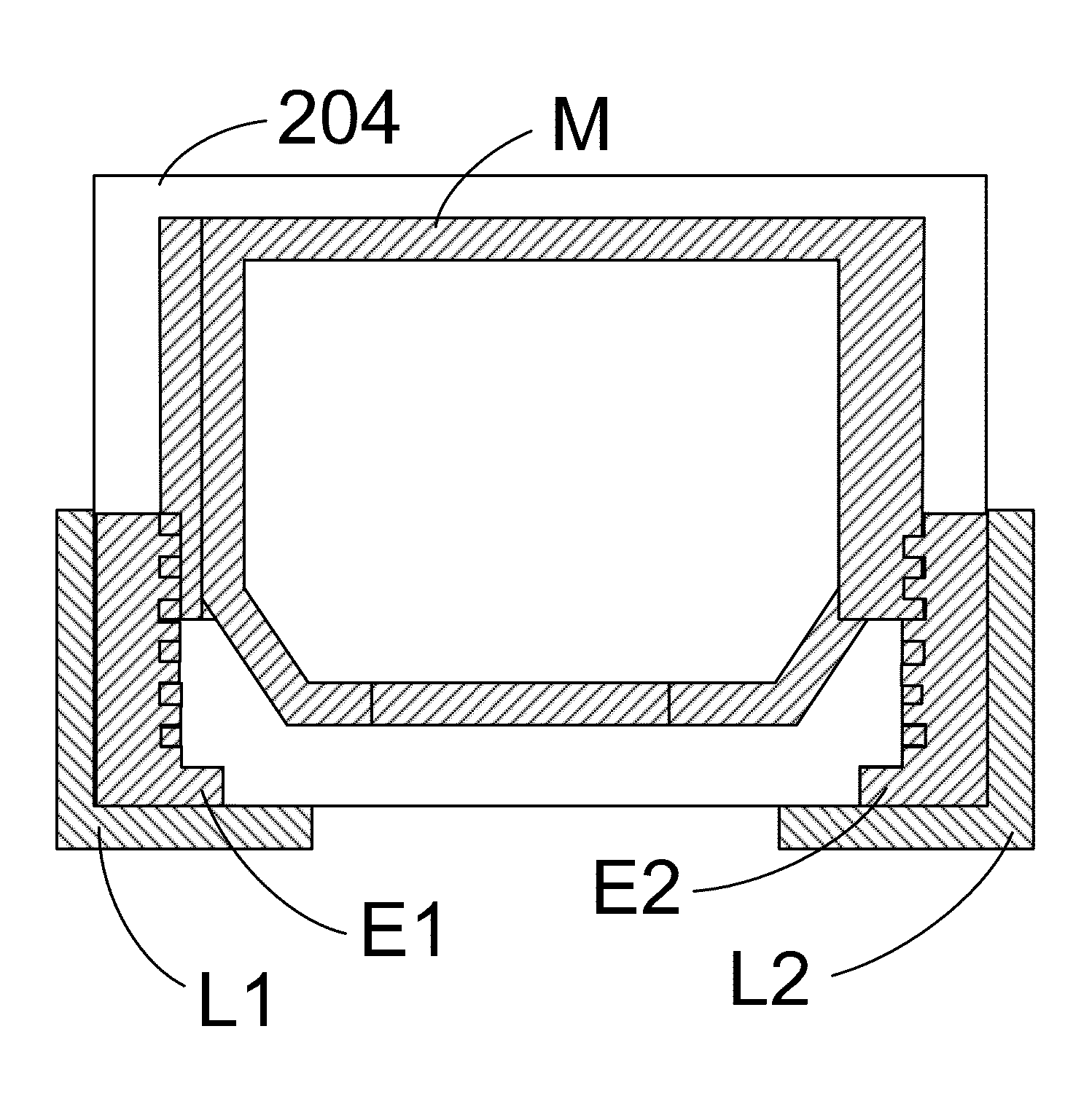
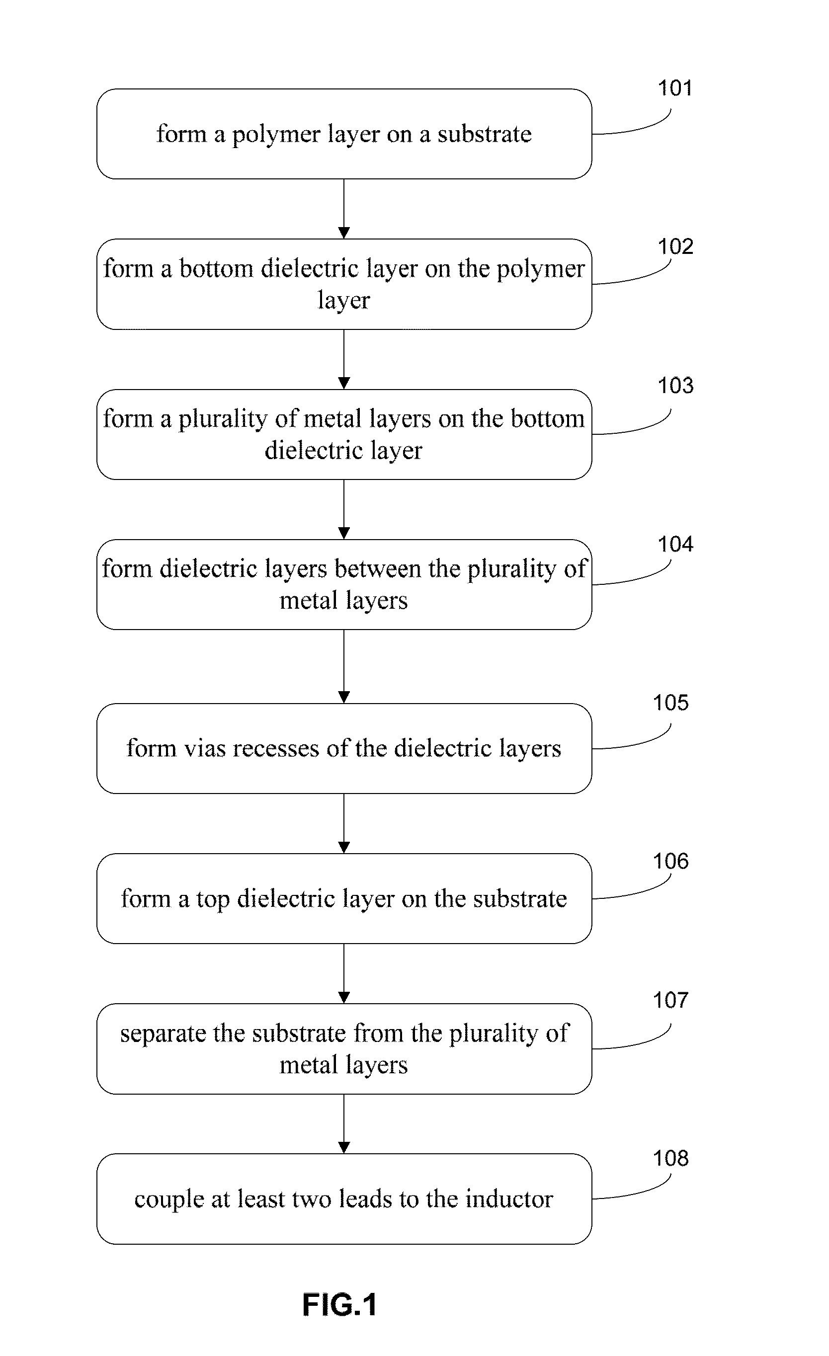
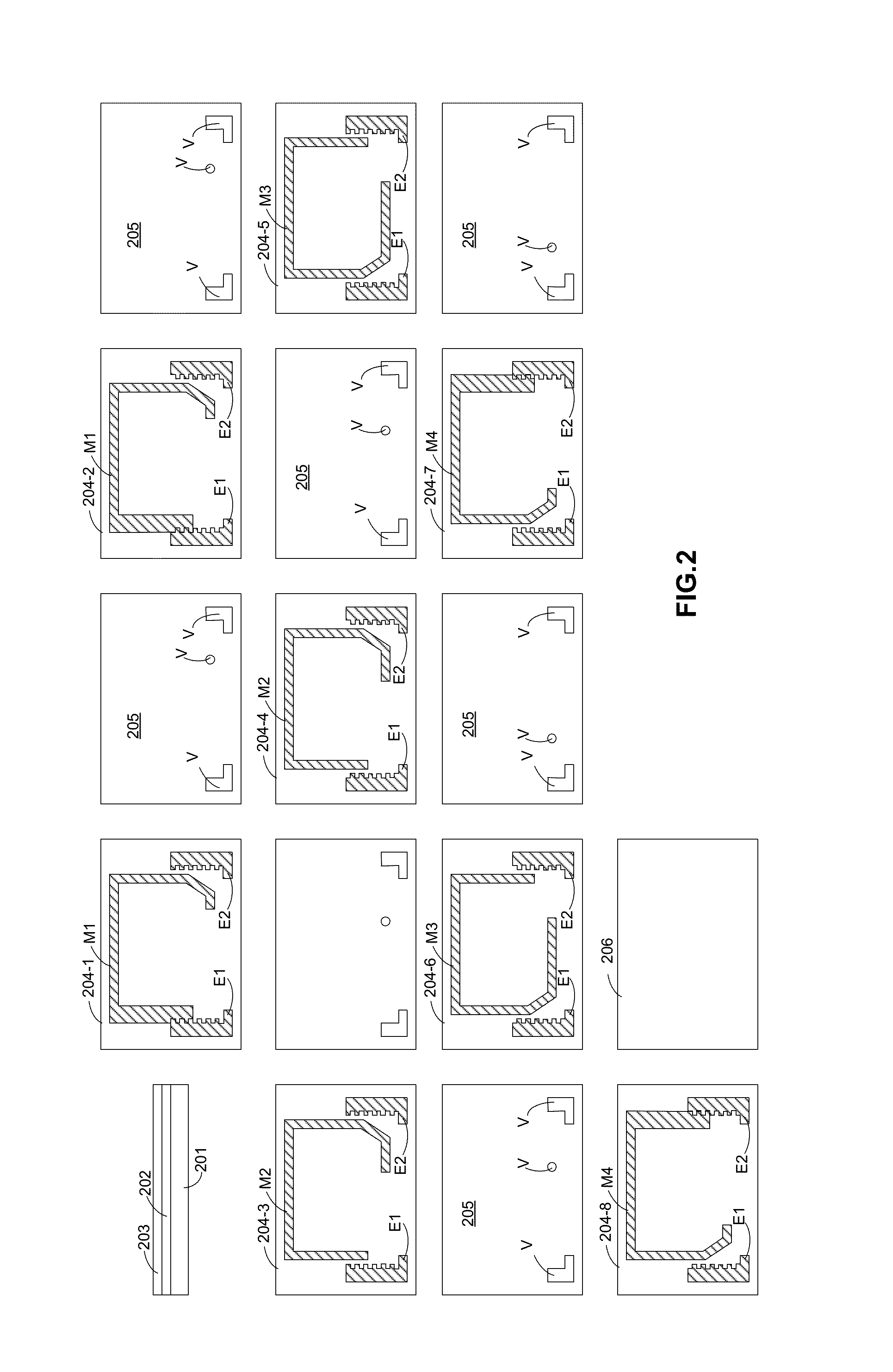
[0034]The present invention discloses a substrate-less electronic component. The substrate-less electronic component can be manufactured by performing film process, such as a lithography process, etching process or thin-film process, on a plurality of conductive layers or insulating layers on the substrate before the substrate is removed. For a device formed on a substrate used for a carrier, the external electrical connection path is often routed along the lateral surface of the substrate or via a through hole so that a longer electrical connection path is needed. Compared to the device formed on the substrate, the thickness of substrate-less device in the present invention is smaller and the device has a better electrical performance.

[0035]The plurality of insulating layers can comprise at least one of epoxy, oxide, a polymer-based material or a magnetic material so that film process, such as a lithography process, etching process or thin-film process, can be applied to the plural...


PUM


Abstract

An electronic component is disclosed, the electronic component comprising: a conductive structure, comprising a plurality of conductive layers separated by a plurality of insulating layers, wherein the plurality of conductive layers and the plurality of insulating layers are stacked in a vertical direction, wherein the plurality of conductive layers forms at least one coil, wherein each of the coil is formed along the vertical direction across said plurality of conductive layers, wherein the plurality of insulating layers are not supported by a substrate.

Description

CROSS-REFERENCES TO RELATED APPLICATIONS[0001]This application claims the benefit of U.S. Provisional Patent Application No. 62 / 079,575 filed on Nov. 14, 2014 and U.S. Provisional Patent Application No. 62 / 083,325 filed on Nov. 24, 2014, which are hereby incorporated by reference herein and made a part of specification.BACKGROUND OF THE INVENTION[0002]1. Field of the Invention[0003]The present invention relates to a method of forming an inductor, and more particularly, a method of forming an inductor using metal layers on a substrate.[0004]2. Description of the Prior Art[0005]A technique for manufacturing a low temperature co-fired ceramic (hereinafter, being referred to as “LTCC”) substrate is a process in which an internal electrode and passive elements (R, L, and C) for given circuits are formed in a green sheet made of glass ceramic by a screen printing method using a metal with high electric conductivity such as Ag, Cu, etc., and a plurality of the green sheets are stacked vert...

Claims


Application Information

Patent Timeline
IPC IPC(8): H01F41/04H01F27/29H01F27/28
CPCH01F41/042H01F2027/2809H01F27/29H01F27/2804H01F27/30H01F27/32H01F27/323H01F27/324H01F41/00H01F17/0013H01F27/292
Inventor TSENG, SHIH-HSIENCHOU, CHIA PEICHIANG, YI-TINGTSAI, CHANG-MING
Owner CYNTEC
Why Eureka
Try Eureka