Method for forming microelectronic assembly

a microelectronic assembly and microelectronic assembly technology, applied in the direction of basic electric elements, electrical apparatus, semiconductor devices, etc., can solve the problems of affecting the performance of the device, affecting the efficiency of the device, so as to reduce the coupling between the coil and the substrate, reduce the possibility of air cavity contamination during subsequent processing steps, and increase the q factor of the inductor

Inactive Publication Date: 2008-09-16
NORTH STAR INNOVATIONS
View PDF8 Cites 3 Cited by
  • Summary
  • Abstract
  • Description
  • Claims
  • Application Information

AI Technical Summary

Benefits of technology

[0007]An apparatus is provided having an inductor with an improved Q factor. The microelectronic assembly comprises a semiconductor substrate having first and second trenches formed thereon, an etch stop layer on the substrate and in the trenches forming first and second etch stop walls, the substrate and the etch stop layer jointly forming a cavity below the etch stop layer and between the first and second etch stop walls with an etch hole interconnecting the cavity and a first surface of the semiconductor substrate, the etch stop layer comprising an etch stop material, an inductor on a second surface of the semiconductor substrate, at least a portion of the inductor being positioned over the cavity in the semiconductor substrate, and a sealing layer formed over the etch hole at the first surface of the semiconductor substrate.

Problems solved by technology

During use, the inductors often experience inductive coupling with the semiconductor material in the substrate, which detrimentally affects the “quality factor,” or “Q factor,” of the inductor and thus impedes the performance of the device.
However, regardless of the thickness of the dielectric, an appreciable amount of coupling still occurs.
Attempts have also been made to create air cavities below the inductors, however the air cavities are not sealed and during subsequent processing steps, such as cleaning and sawing, the air cavity may be contaminated.
Furthermore, it is difficult to control the size and shape of the air cavity.
The air cavity often significantly decreases the mechanical strength of the semiconductor chip, and as a result, the semiconductor chip may be damaged during packaging or shipping.
However, increasing the thickness of the coil increases the size and adds to the manufacturing costs of the device.

Method used


Image

  • Method for forming microelectronic assembly
  • Method for forming microelectronic assembly
  • Method for forming microelectronic assembly

Examples


Embodiment Construction

[0023]The following detailed description is merely exemplary in nature and is not intended to limit the invention or application and uses of the invention. Furthermore, there is no intention to be bound by any expressed or implied theory presented in the preceding technical field, background, brief summary, or the following detailed description. It should also be noted that FIGS. 1-17 are merely illustrative and may not be drawn to scale.

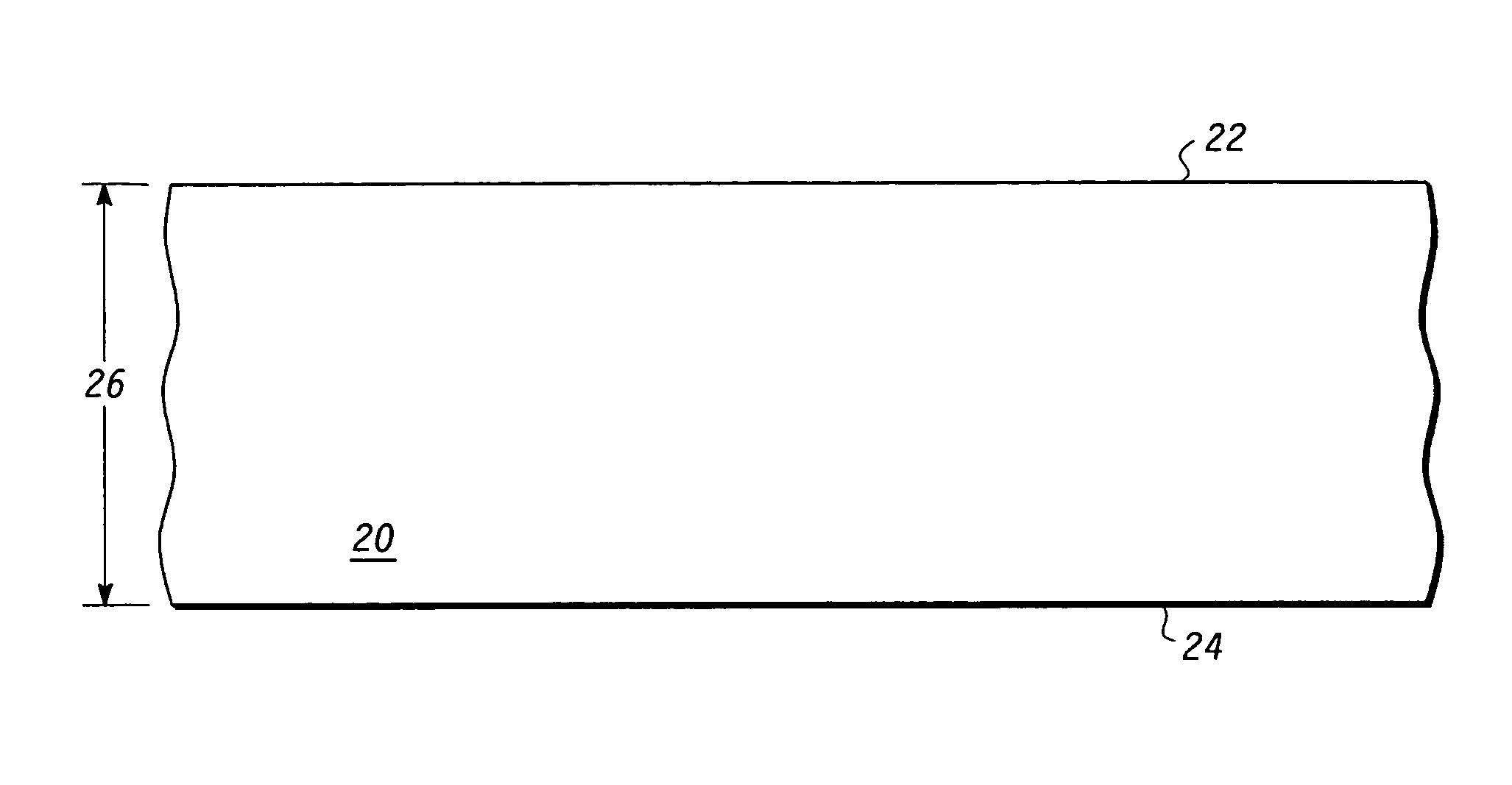
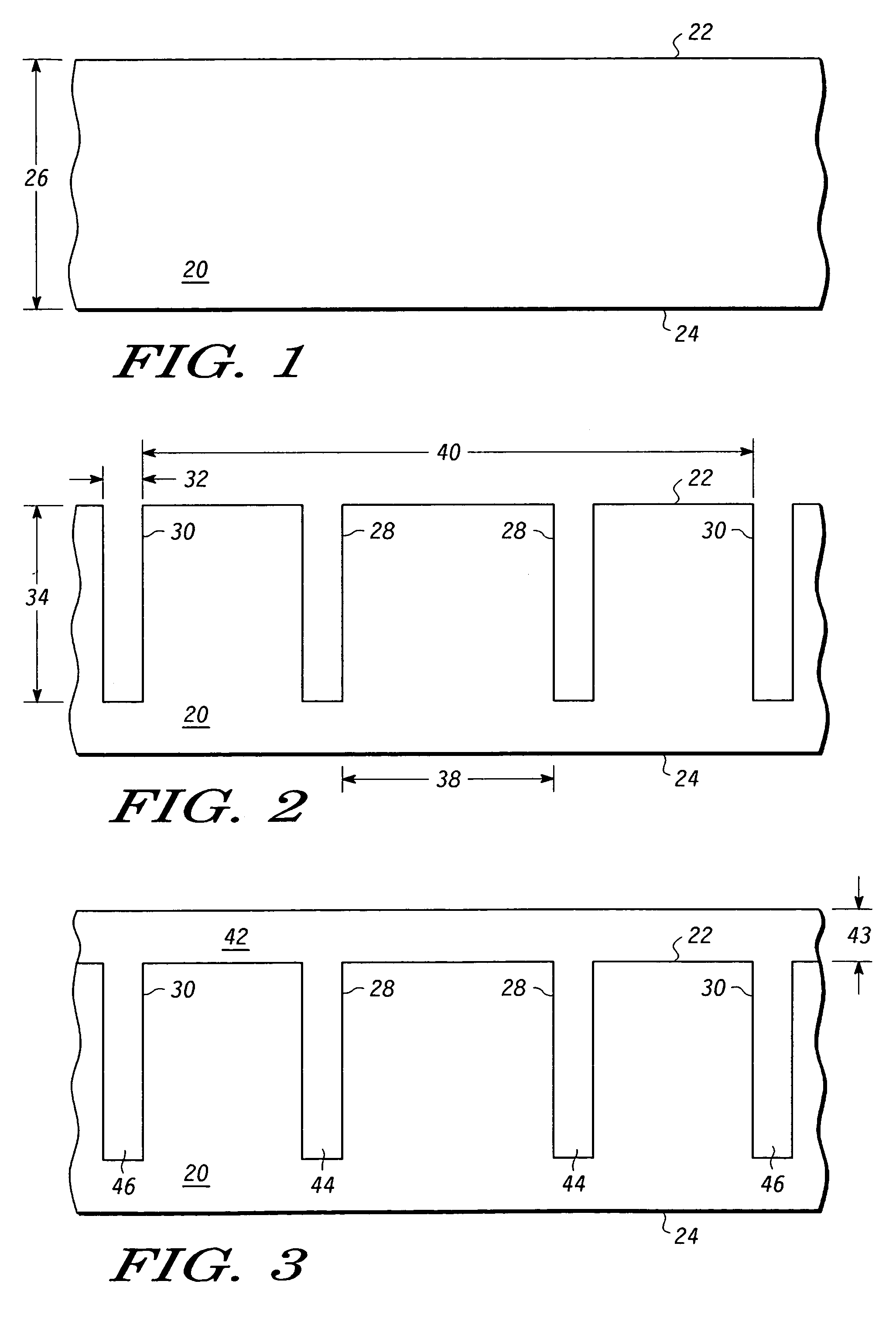
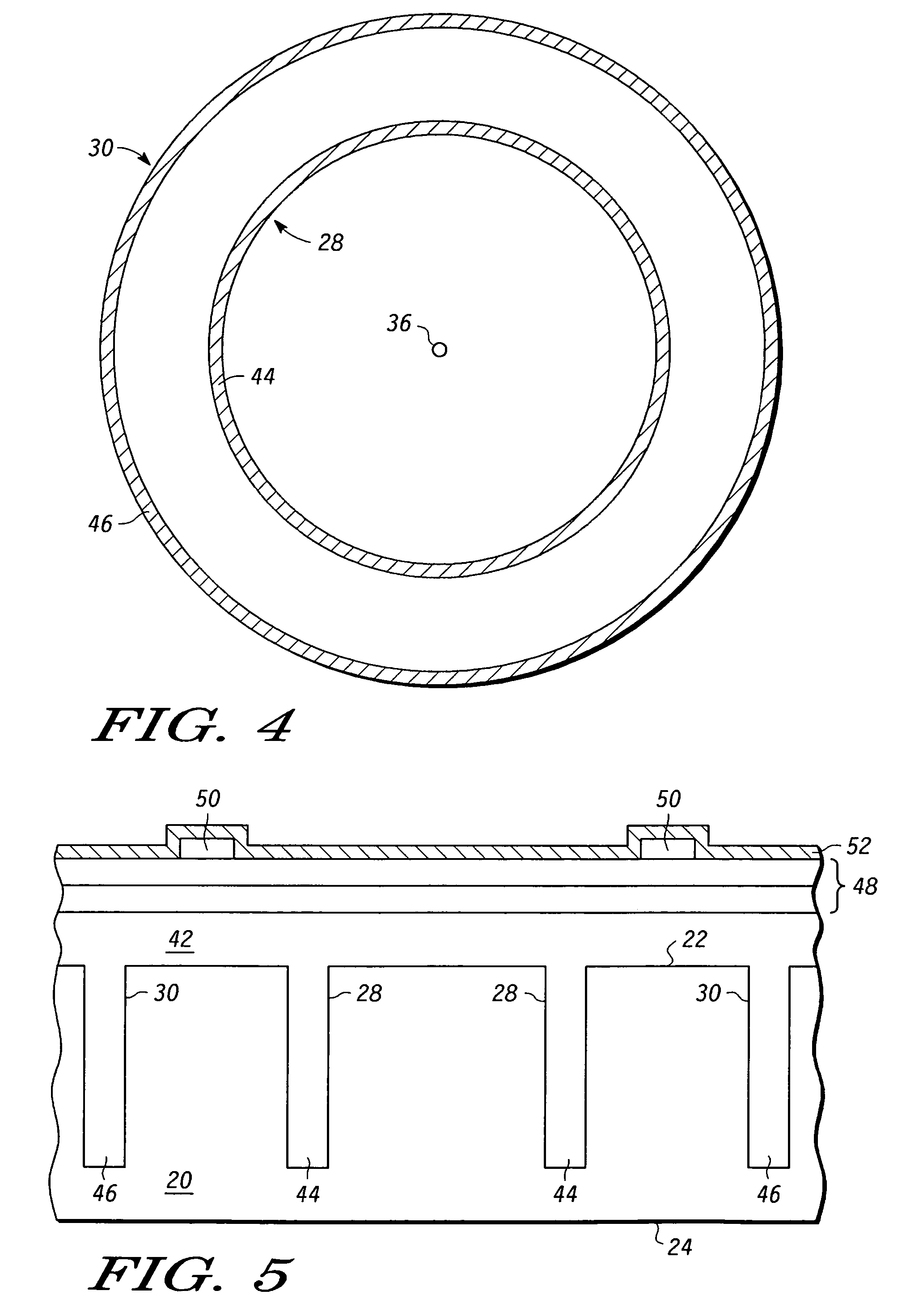
[0024]FIGS. 1-13 illustrate a method for forming a microelectronic assembly including a spiral inductor, according to one embodiment of the present invention. Referring to FIG. 1, there is illustrated a semiconductor substrate 20. The semiconductor substrate 20 is made of a semiconductor material, such as silicon, and includes an upper surface 22 and a lower surface 24. The substrate 20 may have a thickness 26 of approximately 1,000 microns. Although only a portion of the semiconductor substrate 20 is illustrated, it should be understood that the su...


PUM


Abstract

A microelectronic assembly and a method for forming the same are provided. The method includes forming first and second lateral etch stop walls in a semiconductor substrate having first and second opposing surfaces. An inductor is formed on the first surface of the semiconductor substrate and a hole is formed through the second surface of the substrate to expose the substrate between the first and second lateral etch stop walls. The substrate is isotropically etched between the first and second lateral etch stop walls through the etch hole to create a cavity within the semiconductor substrate. A sealing layer is formed over the etch hole to seal the cavity.

Description

FIELD OF THE INVENTION[0001]The present invention generally relates to a microelectronic assembly and a method for forming a microelectronic assembly, and more particularly relates to a method for forming an air cavity beneath a spiral inductor.BACKGROUND OF THE INVENTION[0002]Integrated circuits are formed on semiconductor substrates, or wafers. The wafers are then sawed into microelectronic dies, or semiconductor chips, with each die carrying a respective integrated circuit. Each semiconductor chip is mounted to a package, or carrier substrate, which is often mounted to a motherboard.[0003]The completion of the integrated circuits involves numerous processing steps as well as the formation of various devices on the semiconductor substrate. Depending on the intended use of the semiconductor chip, one of the devices formed on the semiconductor substrate may be an inductor. Spiral inductors are often used in radio frequency (RF) devices and typically include a thin coil of metal form...

Claims


Application Information

Patent Timeline
Patent Type & Authority Patents(United States)
IPC IPC(8): H01L21/8234
CPCH01L21/764H01L27/08H01L2924/0002H01L2924/00H01L29/00H01L27/02H01L21/465
Inventor GOGOI, BISHNU P.
Owner NORTH STAR INNOVATIONS
Why Eureka
Try Eureka