MOS varactor and fabricating method of the same

a technology of varactor and q-factor, which is applied in the direction of semiconductor devices, electrical devices, transistors, etc., can solve the problems of lc tank and vco that employ the device, performance degradation, and q-factor trends of the varactor, so as to improve the performance, improve the q-factor, and reduce the resistance to series

Active Publication Date: 2011-08-02
KOREA UNIV IND & ACADEMIC CALLABORATION FOUND
View PDF5 Cites 3 Cited by
  • Summary
  • Abstract
  • Description
  • Claims
  • Application Information

AI Technical Summary

Benefits of technology

[0009]To overcome the above problem, it is an object of the present invention to provide a MOS varactor with more improved characteristics. In other words, an object of the present invention is to provide a MOS varactor for use in circuits and elements of a millimeter wave frequency band, which has low series resistance and an enhanced Q-factor as compared to a MOS varactor having a multi-finger structure.
[0010]To the end, the present invention provides a MOS varactor which is capable of reducing series resistance, which may be caused by channel resistance and contact resistance, and enhancing a Q-factor by using a plurality of island-like gates seated in a well region of a substrate and gate contacts directly over the gates, and a method of fabricating the MOS varactor.

Problems solved by technology

In this case, although performance deterioration may be mainly problematic as a Q factor of the inductor decides a Q factor of the entire LC tank in a relatively low frequency band of several GHz, the Q factor of the inductor trends to be relatively enhanced while a Q factor of the varactor trends to be rapidly decreased with increase of an operation frequency.
However, such a structure has a fatal drawback in that it suffers from large parasitic resistance leading a low Q factor thereby degrading the performance of the LC tank and VCO that employ the device.

Method used


Image

  • MOS varactor and fabricating method of the same
  • MOS varactor and fabricating method of the same
  • MOS varactor and fabricating method of the same

Examples


Embodiment Construction

[0045]Hereinafter, preferred embodiments of the present invention will be described in detail with reference to the accompanying drawings.

[0046]Prior to the detailed description, it is to be understood that the description and figures mentioned in the specification show the main technical spirit of the present invention, and various structures and techniques known in the art, which may be applied to the present invention based on the main technical spirit of the present invention, are described in brief as possible as they may make the gist of the present invention obscure. However, it is appreciated that such structures and techniques known in the art are apparent to those skilled in the art through the following description.

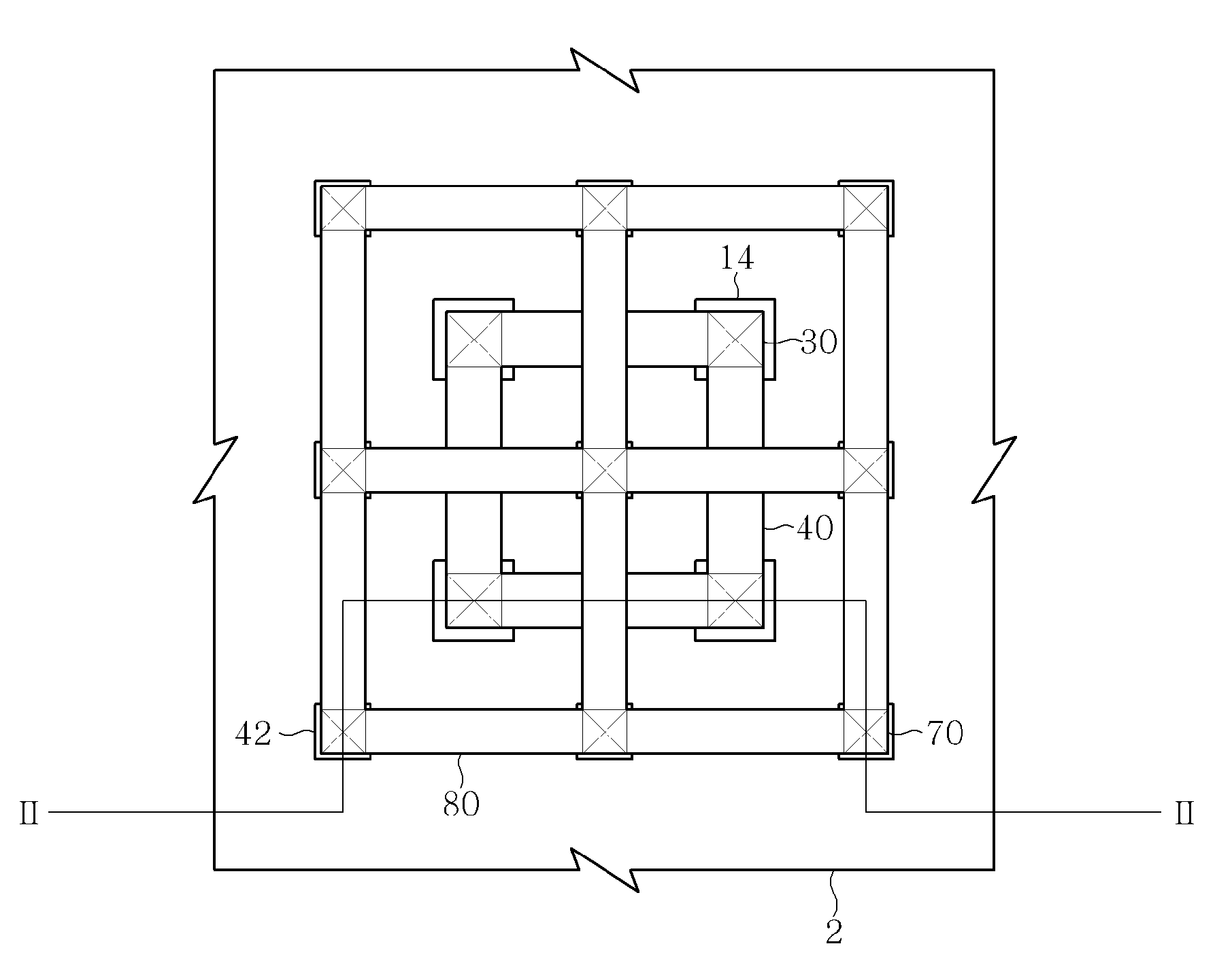
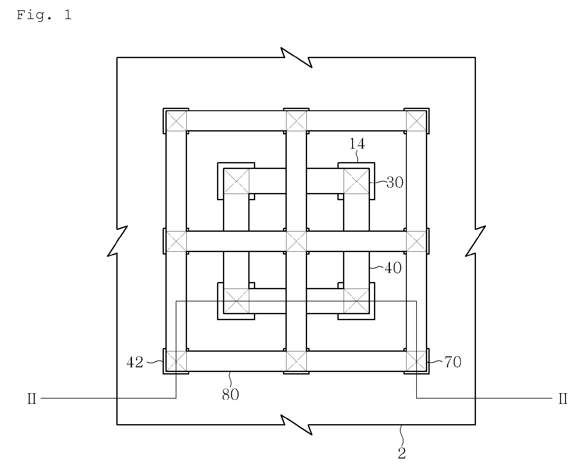
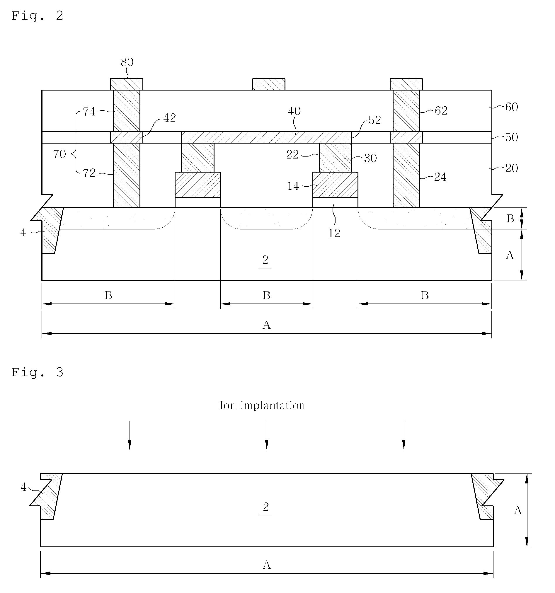
[0047]FIG. 1 is a schematic plan view showing a MOS varactor according to an embodiment of the present invention, and FIG. 2 is a schematic sectional view taken along line II-II of FIG. 1.

[0048]As shown, a MOS varactor according to an embodiment of the present ...


PUM


Abstract

A MOS varactor for use in circuits and elements of a millimeter-wave frequency band, which is capable of reducing series resistance and enhancing a Q-factor by using a plurality of island-like gates seated in a well region of a substrate and gate contacts directly over the gates, includes: gate insulating layers arranged at equal intervals in the form of a (n×m) matrix, and a gate electrode placed on the gate insulating layers in a well region of a substrate; a gate contact which contacts the gate electrode; a first metal wire, which is electrically connected to the gate contact; source / drain contacts arranged at equal intervals in a matrix to form apexes of a square centered at the gate electrode and contact a doping region except for the bottom of the gate insulating layers; and a second metal wire, which is electrically connected to the source / drain contacts.

Description

BACKGROUND OF THE INVENTION[0001]1. Field of the Invention[0002]The present invention relates to a MOS varactor. More particularly, the present invention relates to a MOS varactor for use in circuits and elements of a millimeter-wave frequency band, which is capable of reducing series resistance and enhancing a Q-factor by using a plurality of island-like gates seated in a well region of a substrate and gate contacts directly over the gates, and a method of fabricating the MOS varactor.[0003]2. Description of the Related Art[0004]In pace with recent general trend to information-orientation, many efforts have been made to achieve high speed and high frequencies in the field of wireless communication for high quality wide-band communication services. In this connection, achievement of high integration, high frequency and low noise characteristics of CMOS (Complementary Metal-Oxide Semiconductor) process-based semiconductor devices for RFIC (Radio Frequency Integrated Circuit) has been...

Claims


Application Information

Patent Timeline
Patent Type & Authority Patents(United States)
IPC IPC(8): H01L21/00
CPCH01L29/93H01L29/66174H01L29/94
Inventor RIEH, JAE-SUNGOH, YONG HOKIM, SUE YEONLEE, SEUNG YONG
Owner KOREA UNIV IND & ACADEMIC CALLABORATION FOUND
Why Eureka
Try Eureka