Display Device and Electronic Device

a technology of electronic devices and display devices, applied in thermoelectric devices, instruments, organic semiconductor devices, etc., can solve problems such as inability to operate in circuits, and achieve the effect of high reliability

Active Publication Date: 2016-05-26
SEMICON ENERGY LAB CO LTD
View PDF7 Cites 44 Cited by
  • Summary
  • Abstract
  • Description
  • Claims
  • Application Information

AI Technical Summary

Benefits of technology

[0014]Another object of one embodiment of the present i

Problems solved by technology

Therefore, atmospheric components might enter and lower characteristics of a t

Method used


Image

  • Display Device and Electronic Device
  • Display Device and Electronic Device
  • Display Device and Electronic Device

Examples


embodiment 1

[0128]In this embodiment, structural examples of a display panel are described.

23>

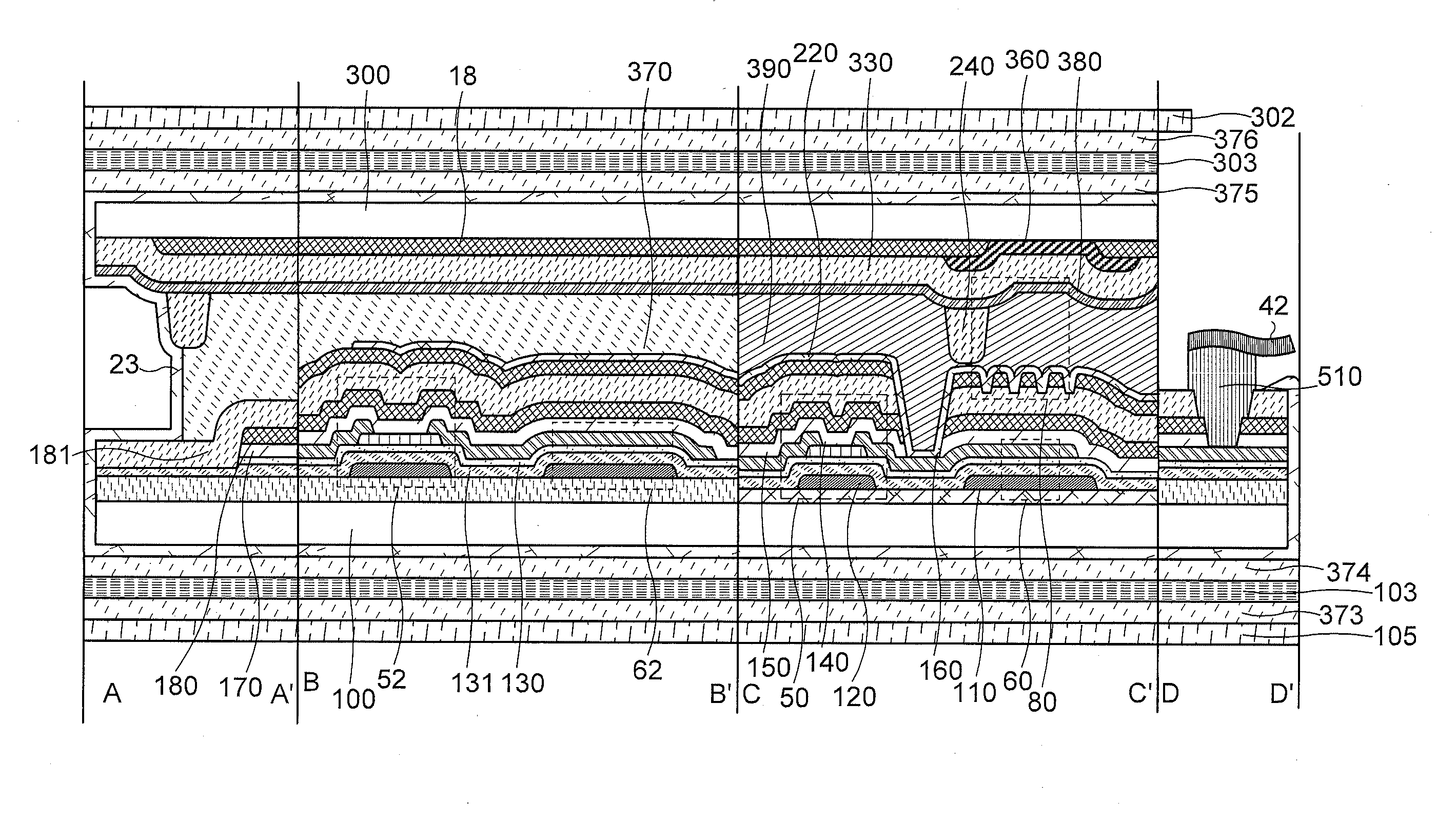
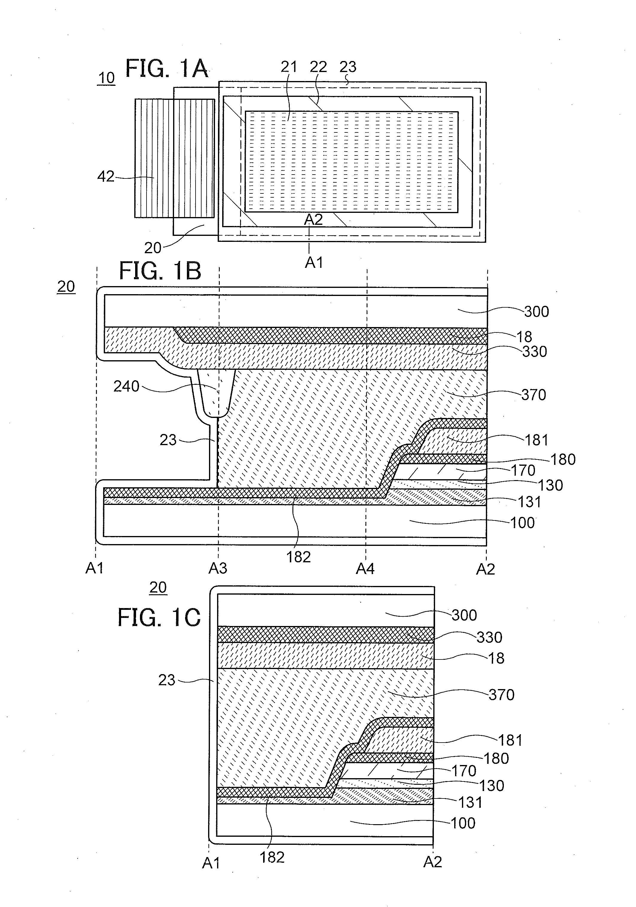
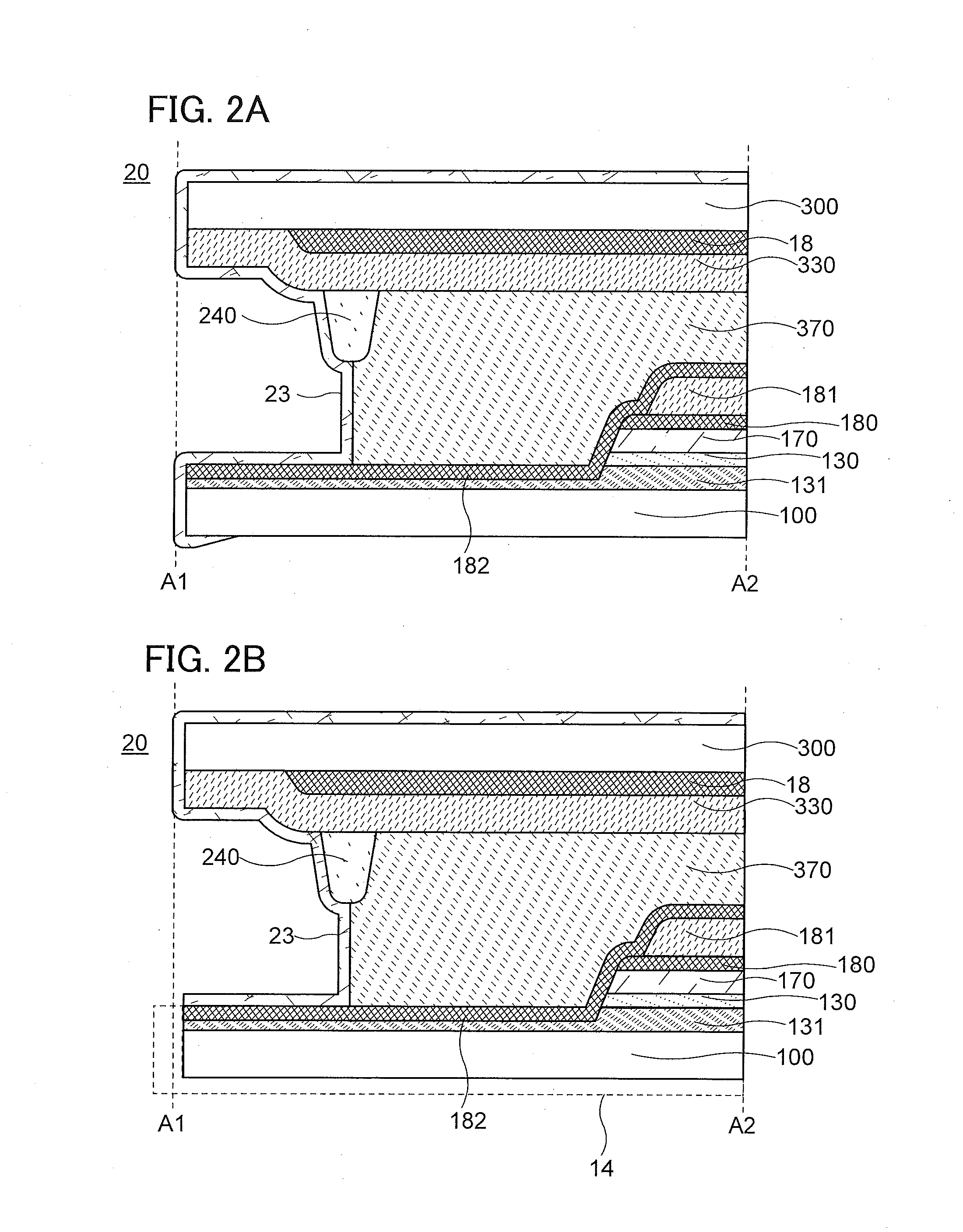
[0129]FIG. 1A is a top view of a display device, and FIGS. 1B and 1C are cross-sectional views thereof. A display device 10 in FIG. 1A includes an FPC 42 and a display panel 20 including a display region 21 and a peripheral circuit 22. In one embodiment of the present invention, a protection film 23 is uniformly formed over the display panel 20. The protection film 23 is preferably formed by an atomic layer deposition (ALD) method. Note that a protection film such as the protection film 23 has a function of, for example, protecting a display element and a transistor, and in some cases has another function of, for example, adding one or more kinds of components to a display element or a transistor. For this reason, the protection film such as the protection film 23 is simply called a film in some cases. For example, the protection film such as the protection film 23 is called a first film, a second film...

embodiment 2

[0153]In this embodiment, a method for manufacturing a plurality of display panels including the protection film 23 described in Embodiment 1 is described.

[0154]FIGS. 7A to 7D illustrate a manufacturing method of the display panel 20. In the schematic views of FIGS. 7A to 7D, a liquid crystal element 80 and the adhesive layer 370 are illustrated as a display element, and a display panel can be formed by bonding an element substrate where a transistor, a capacitor, and the like are provided for the substrate 100 and a counter substrate where a light-blocking layer, a coloring layer, and the like are provided for the substrate 300 to seal liquid crystal. Note that portions similar to those of the manufacturing method in FIGS. 3A to 3C are omitted.

[0155]In a structure including the plurality of display panels 20 (see FIG. 7A), the substrate 300 (an upper side) is cut to form a groove portion 30 (see FIG. 7B). After the formation of the groove portion 30, the protection film 23 is forme...

embodiment 3

>

[0159]A deposition apparatus which can be used for forming a semiconductor layer, an insulating layer, a conductive layer, and the like, which can be used in one embodiment of the present invention, is described below.

>

[0160]In a conventional deposition apparatus utilizing a CVD method, one or more kinds of source gases (precursors) for reaction are supplied to a chamber at the same time at the time of deposition. In a deposition apparatus utilizing an ALD method, precursors for reaction are sequentially introduced into a chamber, and then the sequence of the gas introduction is repeated. For example, two or more kinds of precursors are sequentially supplied to the chamber by switching respective switching valves (also referred to as high-speed valves). For example, a first precursor is introduced, an inert gas (e.g., argon or nitrogen) or the like is introduced after the introduction of the first precursor so that the plural kinds of precursors are not mixed, and then a second pre...


PUM


Abstract

A display device including a peripheral circuit portion with high operation stability. The display device includes a first substrate and a second substrate. A first insulating layer is on a first plane of the first substrate, and a second insulating layer is on a first plane of the second substrate. An area of the first plane of the first substrate is the same as an area of the first plane of the second substrate. The first plane of the first substrate and the first plane of the second substrate face each other. A bonding layer is between the first insulating layer and the second insulating layer. A protection film is in contact with the first substrate, the first insulating layer, the bonding layer, the second insulating layer, and the second substrate.

Description

BACKGROUND OF THE INVENTION[0001]1. Field of the Invention[0002]The present invention relates to a display device and an electronic device.[0003]Note that one embodiment of the present invention is not limited to the above technical field. The technical field of the invention disclosed in this specification and the like relates to an object, a method, or a manufacturing method. In addition, one embodiment of the present invention relates to a process, a machine, manufacture, or a composition of matter. Specifically, examples of the technical field of one embodiment of the present invention disclosed in this specification include a semiconductor device, a display device, a light-emitting device, a power storage device, a memory device, an input device, an input / output device, a method for driving any of them, and a method for manufacturing any of them.[0004]In this specification and the like, a semiconductor device generally means a device that can function by utilizing semiconductor...

Claims


Application Information

Patent Timeline
IPC IPC(8): G02F1/1333G02F1/1368G02F1/1335G02F1/1339H01L51/52H01L27/32
CPCG02F1/133345H01L51/5253H01L51/5246H01L27/322H01L27/3262H01L51/525H01L2251/301H01L27/3265G02F1/133512G02F1/133514G02F1/13394G02F1/1368H01L2251/303H01L51/5284G02F2201/501G02F1/1339H10K71/50H10K59/12H10K50/841H10K50/8426H10K71/851Y02E10/549G02F1/136213G02F1/136222H01L29/7869H01L29/78696H01L27/1225H10K59/38H10K59/124H10K59/1213
Inventor YAMAZAKI, SHUNPEIHIRAKATA, YOSHIHARUISHITANI, TETSUJIKUBOTA, DAISUKEHATSUMI, RYONAKANO, MASARUHAMADA, TAKASHI
Owner SEMICON ENERGY LAB CO LTD
Why Eureka
Try Eureka